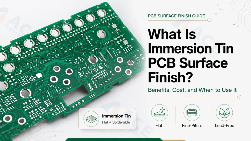
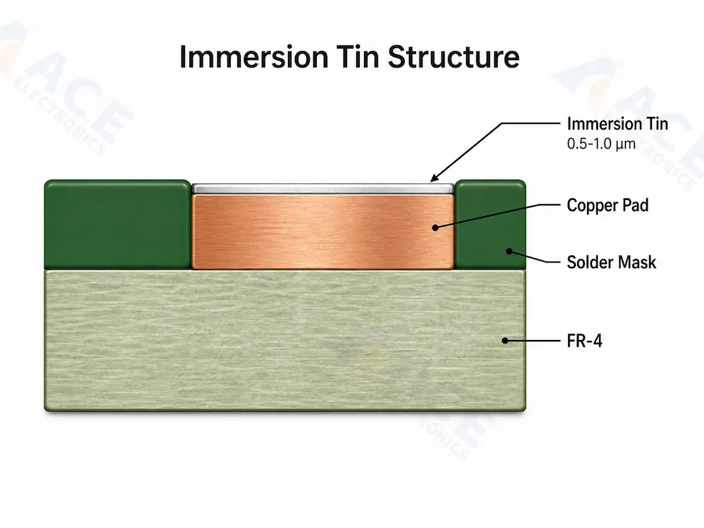
Immersion tin PCB surface finish, also called ImSn or white tin, is a thin tin layer deposited directly over exposed copper pads. It gives the PCB a flat, solderable, lead-free metallic surface for assembly.
Consider to use immersion tin when your PCB needs excellent pad flatness, good solderability, press-fit compatibility, and a mid-cost lead-free finish.
For a broader comparison of surface finish options, read ACE Electronics' guide to PCB surface finish selection. This article focuses only on immersion tin.
Quick Answer: What Is Immersion Tin?
Immersion tin is a chemical PCB surface finish that deposits tin directly on copper through a displacement reaction. The tin layer protects exposed copper from oxidation and provides a solderable surface for PCB assembly.
| Item | Practical answer |
|---|---|
| Full name | Immersion Tin |
| Common abbreviation | ImSn |
| Also called | White tin |
| Finish structure | Copper pad + tin layer |
| Typical tin thickness | 20-40 microinches, about 0.5-1.0 um |
| Common specification reference | IPC-4554 |
| Lead-free | Yes |
| Surface flatness | Excellent |
| Main advantages | Flatness, solderability, press-fit suitability, mid-range cost |
| Main limitations | Limited shelf life, handling sensitivity, tin whisker concern, copper-tin intermetallic growth |
| Best fit | Fine-pitch SMT, BGA/QFN, press-fit connectors, ZIF edge connector interfaces, controlled assembly timing |
Immersion tin is mainly selected as a flat solderable finish. It is also useful for selected connector applications where press-fit insertion or ZIF contact behavior matters.
How Immersion Tin Works on Copper Pads
Immersion tin is deposited directly on copper. During PCB fabrication, exposed copper areas are cleaned and treated in an immersion tin bath. Tin replaces copper at the surface and forms a thin metallic coating.
A simple layer structure:
| Layer | Role |
|---|---|
| Copper pad | Conductive PCB pad or trace surface |
| Immersion tin | Protects copper and provides solderable tin surface |
Typical Immersion Tin Thickness
A common immersion tin thickness range is:
20-40 microinches 0.5-1.0 um
Some fabricators may specify a wider practical range, such as about 0.6-1.2 um, depending on chemistry, customer requirement, and IPC-4554 control.
| Thickness item | Common reference |
|---|---|
| Immersion tin deposit | 20-40 microinches |
| Metric equivalent | About 0.5-1.0 um |
| Wider practical range | About 0.6-1.2 um in some supplier processes |
| Specification reference | IPC-4554 |
| Controlled by | Fabricator process, IPC requirement, OEM drawing note |
When Should You Use Immersion Tin?
Use immersion tin when the PCB needs a flat solderable finish and the assembly schedule is confirmed.
| Project requirement | Immersion tin fit |
|---|---|
| Fine-pitch SMT | Strong fit |
| BGA / QFN / LGA assembly | Strong fit |
| Lead-free soldering | Strong fit |
| Press-fit connectors | Strong fit when connector and process support it |
| ZIF edge connector interface | Good fit in selected designs |
| Lower cost than ENIG | Good fit |
| Long warehouse storage | ENIG may be easier to manage |
| Multiple delayed assembly stages | ENIG may be easier to manage |
| Gold fingers or repeated sliding contacts | Use hard gold |
| Lowest-cost short-cycle SMT | OSP may be better |
A practical selection path:
- Could consider immersion tin for flat solderable pads, fine-pitch assembly, BGA/QFN, and press-fit connector requirements.
- Choose ENIG when the project needs longer storage, wider supply chain flexibility, and stronger appearance stability.
- Choose OSP when the project needs low cost and fast assembly after PCB fabrication.
- Choose hard gold for gold fingers, edge connectors, and repeated-contact areas.
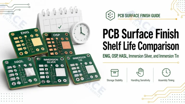
Immersion Tin vs ENIG, OSP, HASL, and Immersion Silver
Each surface finish solves a different engineering problem.
| Finish | Best use | Main advantage | Main limitation |
|---|---|---|---|
| Immersion Tin | Fine-pitch SMT, BGA, press-fit, ZIF interfaces | Flat solderable tin surface, mid cost | Limited shelf life, tin whisker concern, handling sensitivity |
| ENIG | Fine-pitch SMT, BGA, longer storage, broad OEM use | Stable solderability and longer shelf life | Higher cost and nickel layer |
| OSP | Low-cost boards assembled quickly | Low cost and flat surface | Short process window and difficult visual inspection |
| HASL / Lead-Free HASL | Simple boards with larger pads | Low cost and familiar process | Uneven surface, weaker fit for fine pitch and BGA |
| Immersion Silver | RF, high-speed, fine-pitch, controlled assembly timing | Nickel-free and highly conductive | Tarnish and handling sensitivity |
| Hard Gold | Gold fingers and repeated-contact areas | Wear resistance | Higher cost, not a general solder finish |
| ENEPIG | Wire bonding and high-reliability mixed interconnects | Strong reliability and bonding support | Higher cost and less common availability |
For more detail on ENIG, read ACE Electronics' guide to ENIG PCB surface finish. For low-cost controlled assembly timing, see our guide to OSP PCB surface finish. For high-reliability nickel-palladium-gold applications, see our guide to ENEPIG PCB surface finish. For repeated contact surfaces, see our guide to hard gold PCB surface finish.
Shelf Life, Intermetallic Growth, and Handling
Immersion tin has a controlled storage window because copper-tin intermetallic growth continues over time. As the intermetallic layer grows, the remaining pure tin layer becomes thinner, which reduces solderability margin.
A practical shelf-life reference:
| Item | Common guidance |
|---|---|
| Shelf life | Often 3-6 months with proper packaging and storage |
| Best assembly timing | Assemble as soon as practical after fabrication |
| Packaging | Sealed protective packaging |
| Storage | Dry, clean, controlled environment |
| Handling | Gloves required |
| After opening | Move to solder paste printing and assembly within the planned window |
| Inventory control | FIFO recommended |
For production planning, align PCB fabrication, component readiness, SMT scheduling, and incoming inspection before selecting immersion tin.
ENIG gives a wider process window for projects with long storage, multiple warehouse transfers, or uncertain assembly timing. OSP may fit low-cost projects that move quickly from fabrication to assembly.
Tin Whisker Risk
Tin whiskers are small conductive filaments that can grow from tin surfaces under certain conditions. They can create short-circuit risk in sensitive electronics.
Review tin whisker risk for:
- High-reliability electronics
- Automotive electronics
- Medical electronics
- Long-life industrial controls
- Aerospace or defense-related hardware
- Fine-pitch high-density circuits
- Products exposed to mechanical stress or long service life
Tin whisker behavior depends on plating chemistry, deposit structure, stress, storage conditions, board design, and the application environment.
For products where whisker risk is a critical reliability item, review ENIG, ENEPIG, or another finish with the OEM reliability team and PCB fabricator.
Immersion Tin for Press-Fit Connectors
Immersion tin is often used in press-fit connector applications because it provides a uniform tin surface and good hole wall lubricity.
For press-fit projects, review:
- Finished hole size
- Hole tolerance
- Copper plating thickness
- Tin finish requirement
- Connector pin geometry
- Insertion force
- Backplane or connector specification
- Board thickness
- Hole wall quality
- Assembly fixture design
The finish is one part of press-fit reliability. Hole quality, plating thickness, connector pin design, and insertion process should be reviewed together.
A practical fabrication note for press-fit may include:
Surface finish: Immersion Tin per IPC-4554. Finished hole size and tolerance for press-fit connector per drawing. Confirm hole wall plating and insertion requirement before production.
Solder Mask and Fine-Pitch Design Notes
Immersion tin works well with fine-pitch components when solder mask geometry is reviewed before fabrication.
Review these design items before release:
| Design item | Practical guidance |
|---|---|
| Solder mask dam | Use fabricator-approved minimum dam; 127 um is a common reference in many design guidelines |
| Fine-pitch pads | Confirm solder mask registration and mask opening strategy |
| BGA areas | Review pad definition and mask clearance during DFM |
| Plugged vias | Confirm plugging and finish compatibility with the fabricator |
| Peelable mask | Confirm compatibility before using with immersion tin |
| Press-fit holes | Define hole size, tolerance, finish, and connector requirement clearly |
For dense layouts, include immersion tin in the DFM review. This helps align solder mask capability, finish selection, assembly timing, and inspection criteria before production.
What to Specify in PCB Fabrication Notes
For immersion tin, the fabrication notes should define the finish and handling expectations clearly.
Example fabrication note:
Surface finish: Immersion Tin per IPC-4554. Target tin thickness: 20-40 microinches. Boards to be sealed after fabrication. Handle with gloves and assemble within the controlled process window.
For press-fit connector projects:
Surface finish: Immersion Tin per IPC-4554. Press-fit connector holes per mechanical drawing. Confirm finished hole size, hole tolerance, and insertion requirement before production.
For fine-pitch SMT or BGA boards:
Surface finish: Immersion Tin. Review solder mask dam, BGA pad definition, and storage window during DFM. Package boards in sealed protective packaging after fabrication.
The final wording should match your PCB supplier's process and your OEM quality requirement.
What ACE Electronics Usually Recommends
At ACE Electronics, we review immersion tin when a project needs flat solderable pads, lead-free assembly, press-fit compatibility, and lower cost than ENIG.
We usually review immersion tin for:
- Fine-pitch SMT
- BGA, QFN, and LGA assembly
- Press-fit connector boards
- ZIF edge connector interfaces
- Controlled lead-free assembly schedules
- Cost-sensitive designs that still need excellent pad flatness
We usually review ENIG when the project needs longer storage, broader supplier acceptance, and a wider process window.
We usually review OSP when the project needs lower cost and fast assembly after fabrication.
We usually review hard gold when the board has gold fingers, edge connectors, or repeated-contact areas.
For OEM projects, ACE Electronics can review Gerber files, stackup, BOM, connector requirements, press-fit hole specifications, assembly schedule, and storage plan before confirming the surface finish. If you need fabrication support, see our PCB fabrication service.
If you need one supplier to manage PCB fabrication, component sourcing, SMT assembly, testing, and shipment, ACE Electronics also provides turnkey PCBA manufacturing. You can review real project examples in our PCBA case studies.
Final Decision Checklist
Use this checklist before choosing immersion tin.
| Question | If yes |
|---|---|
| Does the design need a flat solderable finish? | Immersion tin is a strong candidate |
| Does the PCB use fine-pitch SMT, BGA, QFN, or LGA? | Immersion tin can fit well |
| Does the project include press-fit connectors? | Immersion tin may be a strong fit |
| Is ENIG too expensive for the project? | Immersion tin may be a practical alternative |
| Can the board be assembled within 3-6 months? | Immersion tin is easier to manage |
| Can boards be handled with gloves and stored correctly? | Immersion tin risk is lower |
| Will the board sit in storage for a long time? | ENIG may be easier to manage |
| Is tin whisker risk critical for this product? | Review ENIG, ENEPIG, or another finish |
| Is the project mainly lowest-cost fast SMT? | OSP may be better |
| Are gold fingers or repeated sliding contacts required? | Use hard gold for those areas |
Immersion tin is a good finish when pad flatness, solderability, and press-fit suitability matter, and when the production flow can control storage and assembly timing.
Final Recommendation
Immersion tin could be one of choice, when your PCB needs a flat, lead-free, solderable finish for fine-pitch SMT, BGA/QFN, or press-fit connector applications.
For long storage, uncertain assembly timing, or high-reliability products where tin whisker risk is a major concern, ENIG or ENEPIG may be easier to manage. For low-cost boards assembled quickly after fabrication, OSP may be the better fit.
If your PCB includes fine-pitch components, BGA/QFN packages, press-fit connectors, or a controlled lead-free assembly schedule, ACE Electronics can help review whether immersion tin is suitable through our PCB fabrication service.
Frequently Asked Questions
What is immersion tin PCB surface finish?
What is immersion tin PCB surface finish?
Immersion tin is a PCB surface finish that deposits a thin tin layer directly over exposed copper pads. It protects copper from oxidation and provides a flat, solderable, lead-free metallic surface for assembly.
What is another name for immersion tin?
What is another name for immersion tin?
Immersion tin is also called ImSn or white tin. The term white tin refers to the appearance of the tin finish on copper pads.
What is the typical thickness of immersion tin?
What is the typical thickness of immersion tin?
A common immersion tin thickness range is 20-40 microinches, or about 0.5-1.0 um. Some suppliers may use a wider practical range such as 0.6-1.2 um depending on process and specification.
Is immersion tin good for fine-pitch components?
Is immersion tin good for fine-pitch components?
Yes. Immersion tin provides excellent surface flatness, so it can work well for fine-pitch SMT, BGA, QFN, LGA, and small passive components.
Is immersion tin suitable for press-fit connectors?
Is immersion tin suitable for press-fit connectors?
Yes. Immersion tin is often considered for press-fit connectors because it provides a uniform tin surface and good hole wall lubricity. Finished hole size, hole tolerance, connector pin design, and insertion force should be reviewed before production.
What is the shelf life of immersion tin PCBs?
What is the shelf life of immersion tin PCBs?
Immersion tin commonly has a shelf life of about 3-6 months when properly packaged and stored. For best solderability, plan assembly as soon as practical after fabrication.
What is the main limitation of immersion tin?
What is the main limitation of immersion tin?
The main limitations are limited shelf life, handling sensitivity, copper-tin intermetallic growth, and tin whisker concern. These risks can be managed with proper finish selection, packaging, storage, and production timing.
Does immersion tin have tin whisker risk?
Does immersion tin have tin whisker risk?
Yes. Tin whiskers can grow from tin surfaces under certain conditions. For long-life or high-reliability products, review tin whisker risk with the OEM reliability team and PCB fabricator before choosing immersion tin.
Is immersion tin better than ENIG?
Is immersion tin better than ENIG?
Immersion tin is better when the project needs a flat lead-free finish, press-fit suitability, and lower cost than ENIG within a controlled assembly window. ENIG is better when the project needs longer storage, broader supplier acceptance, and a wider process window.
Is immersion tin better than OSP?
Is immersion tin better than OSP?
Immersion tin provides a metallic tin surface and excellent flatness. OSP is usually lower cost and works well for fast assembly. Choose immersion tin when the project needs a flat metallic finish or press-fit compatibility; choose OSP when cost and quick assembly are the main priorities.
Is immersion tin RoHS compliant?
Is immersion tin RoHS compliant?
Yes. Immersion tin is a lead-free PCB surface finish and is suitable for RoHS-compliant assembly.
What fabrication note should I use for immersion tin?
What fabrication note should I use for immersion tin?
A practical note is: "Surface finish: Immersion Tin per IPC-4554. Target tin thickness: 20-40 microinches. Boards to be sealed after fabrication. Handle with gloves and assemble within the controlled process window." Adjust the final wording to match your supplier and OEM requirements.
About the Author
Bill Ho is Sales Engineer and Chief Editor at ACE Electronics, with 10 years of experience in PCB fabrication and PCB assembly.
He writes practical technical content focused on manufacturability review, fabrication communication, and assembly risk reduction.