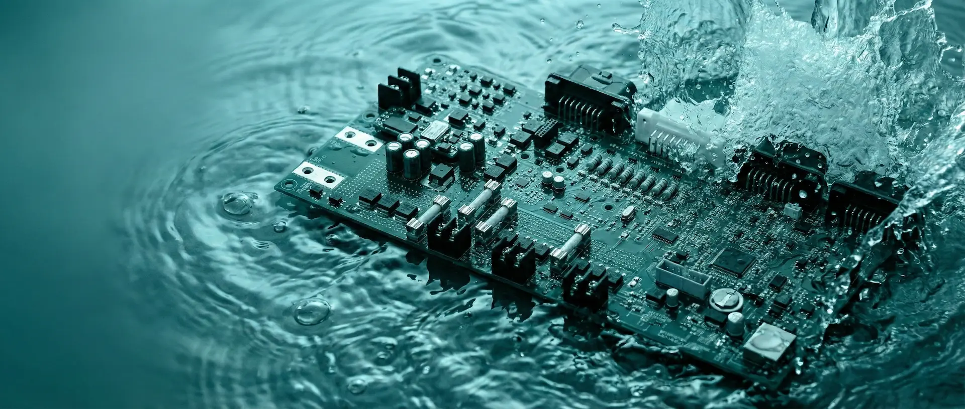
PCBA Solution–
Parylene Coating Service
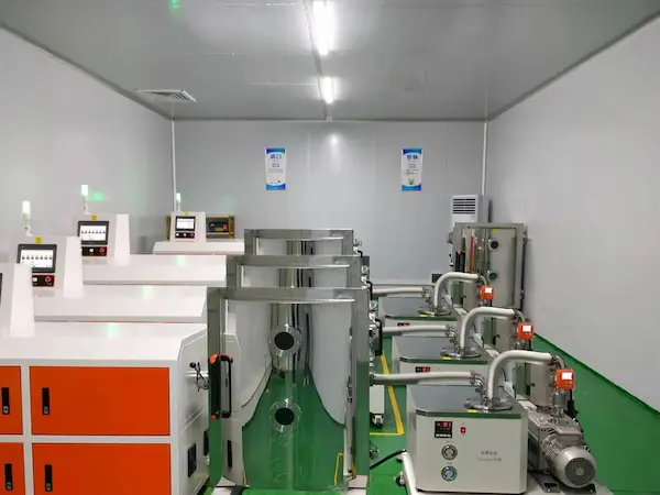
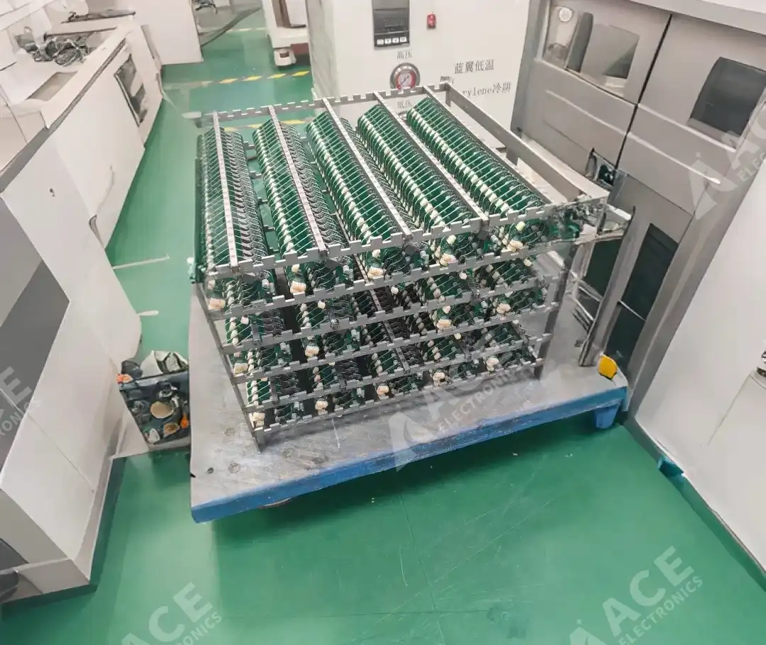
ACE Electronics provides in-house parylene CVD coating for PCB assembly, including masking, thickness control, inspection, and post-coating testing support.
- Reduce moisture and corrosion risk in high-density assemblies with conformal, low-permeability coverage
- Protect fine-pitch areas, wire bonds, and hidden gaps without the pooling or edge-thinning common in liquid coatings
- In-house processing eliminates the quality risks of supplier transitions, keeping your coating specs locked in from day one.
Parylene creates a thin, uniform protective film for assembled PCB that are hard to coat evenly with liquid materials
Unlike spray, brush, or dip-applied liquid coatings, parylene is deposited from vapor. That helps it wrap around edges, fine gaps, and densely packed features more evenly while keeping the film very thin.
It is commonly chosen when coverage consistency, low added thickness, moisture protection, or electrical sensitivity matters more than simple surface-only coating.
Uniform coverage
Helps reach corners, under leads, and around dense geometry.
Very thin film
Useful when tight tolerances or sensitive assemblies limit coating build.
Complex assemblies
Often chosen when liquid coating may pool, bridge, or miss hidden surfaces.
Key Benefits of Parylene Coating
Parylene is often chosen when assembled PCB need thin, even coverage across dense geometry, hidden surfaces, or electrically sensitive areas.
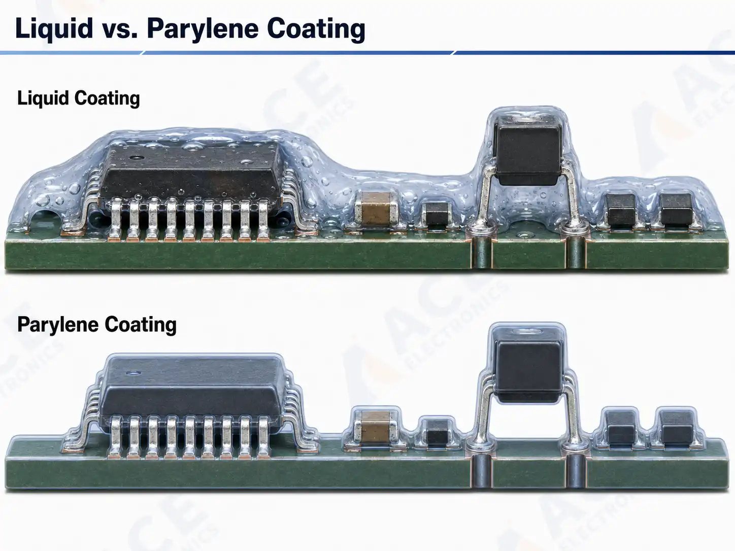
Liquid coating can build up more heavily on exposed surfaces and more lightly in hidden areas. Parylene is deposited from vapor, which helps create a thinner and more even film across more of the assembly.
Uniform coverage on complex geometry
Because parylene is deposited from vapor rather than applied as a liquid, it is better suited to coating edges, fine gaps, vertical surfaces, and hard-to-reach features with a more even film.
Thin protection with low material build
Parylene is often selected when the assembly has tight spacing or limited tolerance for coating thickness, because protection can be added with far less buildup than many liquid-applied alternatives.
Strong moisture and environmental barrier
Parylene is widely used when assemblies need reliable protection against moisture, contamination, and general environmental exposure without covering the board in a thick encapsulating layer.
Suitable for electrically sensitive assemblies
For signal-sensitive, miniaturized, or performance-critical electronics, parylene is often preferred when designers want protection while keeping added mass and film build to a minimum.
What We Coat and How We Run It
Choose the Outcome Your Projects Need
Moisture and corrosion protection
Best for: outdoor, condensation, salt exposure, long service life
What we deliver
- • Conformal coating coverage plan, selective masking, photo checkpoints
- • Record package options including run ID and material traceability
What we need
Environment description, exposure type, target lifetime, keep-out areas
Electrical insulation and leakage risk reduction
Best for: higher voltage spacing concerns, contamination sensitivity
What we deliver
- • Thickness target aligned to voltage and spacing risk
- • Optional witness coupon checks and dielectric-focused inspection points
What we need
Voltage range, creepage and clearance constraints, critical nets list
RF-friendly protection for sensitive electronics
Best for: RF modules, antennas, low-loss requirements
What we deliver
- • Thin-film strategy and keep-out alignment for tuned areas
- • Coating impact review based on your geometry and constraints
What we need
Frequency band, sensitive zones, any tuned structures, allowed thickness range
Next is the exact 5-step workflow and the deliverable at each step.
Our 5-Step In-house Parylene Coating Workflow
How Parylene C Protects Hydrogen Forklift Control Boards
A practical example of how ACE handled PCBA manufacturing, functional testing, and in-house parylene coating for boards used in harsh industrial environments.
Application
Hydrogen forklift control boards used in demanding industrial operating conditions.
What the build included
PCB assembly, functional testing, keep-out planning, and final in-house Parylene C coating.
Why this case matters
It shows where thin moisture-resistant protection and better control over masking and release checks become important in real production.
Quality Evidence Options You Can Request
01 Standard evidence
- Traveler with routing steps, run ID, lot traceability
- Visual inspection checkpoints with photo set for key areas
- Masking and keep-out confirmation records
02 Optional evidence for higher-risk programs
- Thickness verification via witness coupons, defined sampling plan
- Adhesion verification approach aligned to your acceptance method
- Focused inspection on connectors, test pads, high-density zones
03 Change control and acceptance alignment
- Any changes in material type, thickness target, masking method, or cleaning route follow a documented approval path
- Acceptance criteria are aligned early with reference photos and inspection points to reduce receiving disputes
Keep Parylene Process in the Same Factory
When assembly, testing, and parylene coating stay in the same production flow, keep-out changes, fit issues, and inspection points are easier to confirm before shipment instead of being passed between suppliers.
What this simplifies
-
1
One production flow
Assembly, testing, coating, and release stay on the same traveler.
-
2
Faster masking feedback
Keep-out, connector opening, and fit issues can be checked earlier.
-
3
Inspection aligned earlier
Coverage photos, thickness checks, and shipment records can be planned with the build.
What We Need for a Parylene Quote
Assembly files and keep-out areas
3D files, PCB drawings, or marked PDFs showing connectors, no-coat zones, and fit-critical surfaces.
Coating scope and thickness target
Whether you need full coverage or selective coating, plus any thickness limits for RF areas or tight interfaces.
Operating environment
Humidity, condensation, salt exposure, chemicals, temperature range, and expected service life.
Electrical or RF constraints
Voltage range, sensitive nets, tuned structures, antenna areas, or low-loss requirements if they matter.
Quantity, delivery plan, and acceptance needs
Prototype or volume quantity, shipment timing, and any inspection records or verification points you need at receiving.
Request a Parylene Coating Review
Send your assembly files and coating requirements. We will review keep-out areas, thickness fit, and any points that may affect cost, lead time, or inspection.
Parylene Coating FAQs
Q
What is Parylene coating and how does it differ from liquid coatings?
What is Parylene coating and how does it differ from liquid coatings?
Parylene (poly-para-xylylene) is a vacuum-deposited polymer that forms an ultra-thin, pinhole-free protective layer through Chemical Vapor Deposition (CVD). Unlike liquid acrylics or silicones that are sprayed or dipped, Parylene grows molecule-by-molecule in a vacuum chamber, resulting in truly conformal coverage with no pooling, bridging, or thin spots—even under components and inside tight spaces.
Q
How thick is Parylene coating and why does thickness matter?
How thick is Parylene coating and why does thickness matter?
Parylene coatings range from 0.1 to 50 microns, with 5-25 microns being standard for electronics. Unlike thicker liquid coatings, Parylene provides excellent dielectric protection and moisture barrier properties at just 5-10 microns—critical for miniaturized medical devices and microelectronics where added mass or dimensional change must be minimized.
Q
What are the key advantages for electronics protection?
What are the key advantages for electronics protection?
Parylene offers exceptional dielectric strength (7,000V/mil), complete moisture barrier (WVTR <0.1 g·mm/m²·day), and solvent/chemical resistance without adding thermal stress. It's transparent, UV-stable, and operates from -200°C to +200°C. Most importantly, it provides USP Class VI / ISO 10993 biocompatibility for medical implants and FDA-regulated devices.
Q
How is the CVD application process performed?
How is the CVD application process performed?
The process occurs in a specialized vacuum chamber at room temperature: (1) Raw dimer powder is heated to 150°C to vaporize; (2) Pyrolysis at 680°C cleaves the dimer into monomer gas; (3) Monomer enters the deposition chamber and polymerizes spontaneously on all exposed surfaces. No solvents, catalysts, or curing ovens are required, eliminating thermal stress on sensitive components.
Q
Does Parylene require primer or adhesion promotion?
Does Parylene require primer or adhesion promotion?
While Parylene adheres well to clean metals, ceramics, and most plastics, we apply silane-based adhesion promoters (A-174) for noble metals (gold, silver) or low-surface-energy materials like silicone rubber. We also use plasma surface activation for critical medical devices to ensure coating retention during autoclave sterilization or long-term implantation.
Q
Can Parylene coating be repaired or removed for rework?
Can Parylene coating be repaired or removed for rework?
Parylene cannot be dissolved by common solvents, making localized rework challenging. Removal requires mechanical abrasion (micro-blasting), laser ablation, or thermal methods. For components requiring occasional repair, we recommend designing selective coating barriers or using peelable masks during deposition to keep connector areas uncoated.
Q
Why is Parylene more expensive than other conformal coatings?
Why is Parylene more expensive than other conformal coatings?
Higher costs stem from (1) specialized vacuum deposition equipment and batch processing limitations; (2) Raw dimer material costs significantly more than acrylic/urethane resins; (3) Masking labor is intensive since all surfaces get coated; and (4) Processing time is longer due to vacuum cycles. However, for high-reliability medical, aerospace, or implant applications, the cost-per-device is justified by unmatched protection levels.
Q
Which industries typically specify Parylene coating?
Which industries typically specify Parylene coating?
Primary applications include: Medical (pacemakers, neurostimulators, hearing aids requiring biocompatibility); Aerospace/Defense (circuit boards in satellites and avionics exposed to extreme temperatures); Automotive (sensors in engine compartments); Consumer Electronics (hearing aids and wearables needing moisture protection); and MEMS devices where stiction prevention is critical.
What to Clarify Before Parylene Coating
Parylene Tech Guides
Parylene Conformal Coating for PCB Assembly
Parylene conformal coating is a vapor-deposited protective film used on PCB assemblies that need very uniform coverage, strong moisture protection, and reliable barrier performance on dense or complex boards.
Read Guide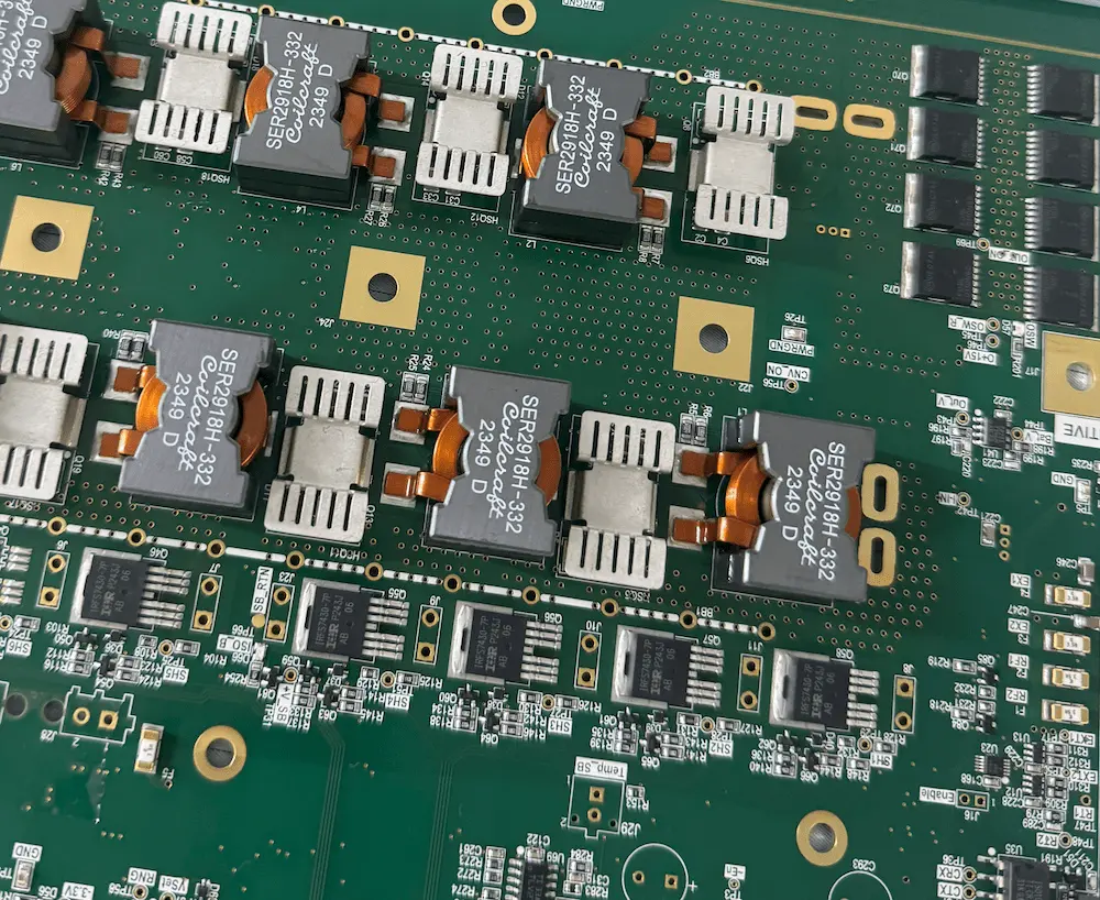
Parylene C Coating for PCB Assembly
Parylene C coating is a vapor-deposited conformal coating widely used on PCB assemblies and electronics because it combines a strong moisture barrier, stable dielectric insulation, and very uniform thin-film coverage.
Read Guide
Parylene N Coating for PCB Assembly
For many RF and signal-sensitive PCB assembly, Parylene N coating is one of the first coating types engineers review when low dielectric loading and very low energy loss in the coating layer matter.
Read GuideStart Your Projects Manufacturing Today!
Whether you need a quick quote or technical consultation, we're here to help.
Quick Response via WhatsApp
Get instant answers to your questions
Connect directly with our technical team for immediate assistance.
We typically respond within 30 minutes during business hours.
Business Hours: Mon-Fri 9:00-18:00 (GMT+8)