
On this page
Hydrogen forklift control boards operate in demanding industrial environments. In cold-chain warehouses, industrial storage, and high-humidity logistics, these electronics boards face condensation, dust, temperature cycling, and electrical stress over long service periods. Standard PCB assembly alone is rarely enough—the board protection strategy must be built into manufacturing from the start.
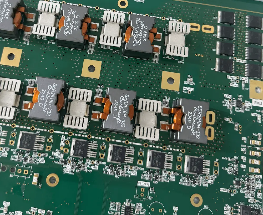
In a long-running project for a U.S. customer, we delivered hydrogen forklift control boards through a turnkey workflow: PCB fabrication, component sourcing, cleaning, masking, in-house Parylene C coating, and final inspection. The customer name under NDA. What we can share is the engineering side: why Parylene C was chosen, which process risks had to be controlled, and how this approach fits similar high-reliability industrial PCB projects.
Project Snapshot
| Item | Details |
|---|---|
| Customer | U.S. customer under NDA |
| Main application | Hydrogen forklift control boards |
| Cooperation length | ~10 years |
| Scope | PCB fabrication, sourcing, PCBA, functional testing, cleaning, masking, in-house Parylene C coating, final inspection |
| Main goals | Moisture protection, corrosion resistance, insulation, long-term reliability |
| Extra support | DFM review, BOM risk control, cost optimization, connector substitution planning |
Why Parylene C Coating
The protection material for this project was Parylene C. The goal was moisture resistance, corrosion protection, insulation, and long-term stability on control boards used in a demanding industrial environment.
Parylene C fit the application for several reasons:
- Thin, uniform, vapor-deposited protective layer
- Reaches complex board geometries more consistently than liquid-applied alternatives
- Supports insulation performance where condensation risk is a concern
- Adds protection without the thick build-up associated with heavier coating systems
| Parameter | Specification | Reference / Test Method |
|---|---|---|
| Base Material | Parylene C | Project material specification |
| Target Thickness | 25 µm | Based on project coating requirement |
| Dielectric Strength | Typical 5,600 V/mil | ASTM D149 |
| Operating / Service Temperature | Suitable for –160°C to 100°C | Temperature cycling test / supplier datasheet |
| Coverage Characteristic | Uniform, continuous conformal film over complex geometries | Visual inspection and process validation |
Material properties:
- Conformal coverage over sharp edges, lead frames, and trace corners via molecular-level vapor deposition
- Transparent, thin, and uniform—suitable for high-reliability electronic protection
- No thermal curing step after deposition, reducing thermal stress on sensitive assemblies
The Main Challenges for This Project
1. Cleaning after assembly
Contamination left on the board after assembly—flux residue, surface oils, handling residue—can cause adhesion failure, blistering, or delamination under the coating.
We treated cleaning as a important process step. The board had to reach deposition clean enough to support reliable film adhesion.
2. Masking around connectors and functional areas
Standard tape was not enough. We used custom masking fixtures and boots for connector interfaces. This sealed critical areas tighter, reduced unwanted vapor penetration, and improved repeatability across builds.
3. Long-term sourcing pressure
This assembled PCB used major semiconductor and power-device brands, with connector cost and availability pressure. In a long-running contract electronics manufacturing, sourcing means continuity, BOM stability, and practical substitution planning—not just placing orders.
We combined BOM risk review, cost optimization, and connector replacement planning to keep the supply being stable without reducing quality control.
4. Process coordination across multiple steps
When a project spans PCB fabrication, sourcing, pcb assembly, testing, cleaning, masking, coating, and inspection, each handoff adds a chance for delay or inconsistency. Splitting these steps across multiple vendors compounds the risk.
This project stayed inside one connected manufacturing path—from bare PCB through protected finished assembly.
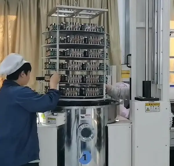
Our Turnkey Manufacturing Process
We manage the entire production chain in-house through eight stages:
-
PCB Fabrication
12 layers boards with controlled impedance for power circuits -
Component Sourcing
Authorized distribution channels with active BOM risk monitoring -
SMT & THT Assembly
Automated placement with optimized thermal profiles -
Functional Testing
These assembled PCBs were Functional Tested before coating -
Precision Cleaning
Ultrasonic wash followed by deionized water rinse -
Selective Masking
Custom silicone fixtures for connectors and test points -
Parylene C Deposition
Apply Parylene C coating on the assembled PCB (25 micron thickness) -
Final Inspection
Visual verification, thickness measurement, final electrical testing
All stages stay inside our facility, no inter-supplier handoff risks.
We also supported DFM review, BOM risk control, and components cost optimization before production began.
What Can Go Wrong Without The Parylene C Coating
In hydrogen forklift environments, condensation repeatedly forms on PCB surfaces. When this moisture meets ionic contamination on an energized board, electrochemical migration begins. Over time, this creates dendrite growth and leakage paths.
Unprotected or poorly coated PCBs fail early when condensation and contamination occur together. Low-grade coatings only delay the problem. Once the coating cracks, moisture enters and damage continues.
| Risk Factor | Standard Conformal Coating | Parylene C Vapor Deposition |
|---|---|---|
| Moisture Ingress Pathways | High risk at brush stroke boundaries and edges | Pinhole-free barrier with uniform edge coverage |
| Ionic Contamination Risk | Residue may migrate under coating film | Contamination fully encapsulated and isolated |
| Condensation Tolerance | Degradation observed within 6–12 months in cycling environments | No measurable degradation after 5+ years field exposure |
| Rework Complexity | Solvent removal possible | Requires mechanical abrasion for repair |
Comparative data based on 10-year field monitoring in hydrogen forklift applications.
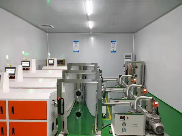
Why One-Stop Assembly Worked
The value we provided to our client, is keeping components sourcing, pcb assembly, cleaning, masking, parylene coating, and inspection connected in one controlled workflow.
That gave the customer:
- One manufacturing path from bare PCB to protected assembly
- Fewer handoff risks between process steps
- Tighter coordination between assembly and coating
- Better control of high-risk connector and no-coat areas
- A practical long-term production model for a demanding application
Conclusion
In this project, Parylene C was part of a full workflow: PCB fabrication, sourcing, assembly, testing, cleaning, masking, coating, and final inspection.
Consider Parylene coating if your application meets three or more of these:
- [ ] Device operates outdoors or in uncontrolled humidity
- [ ] Regular thermal cycling between -20°C and +60°C
- [ ] Field failure would create safety risk or downtime costs exceeding $10,000
- [ ] PCB contains fine-pitch components with gaps below 0.5 mm
- [ ] Previous field failures show evidence of corrosion or dendritic growth
- [ ] Design requires 10+ year service life without maintenance access
For other protection methods such as conformal coating, see our conformal coating selection guide and conformal coating service.
Submit your Gerber files and BOM for a complimentary DFM review.
Frequently Asked Questions
Why use Parylene C on hydrogen forklift control boards?
Why use Parylene C on hydrogen forklift control boards?
Parylene C improves moisture resistance, corrosion protection, insulation, and long-term reliability in demanding environments.
Why does cleaning matter before Parylene C coating?
Why does cleaning matter before Parylene C coating?
Residue left on the board reduces adhesion quality and long-term coating reliability.
What is the biggest masking risk on a Parylene C-coated control board?
What is the biggest masking risk on a Parylene C-coated control board?
Masking the many automotive-style connector areas that must remain coating-free.
What thickness range is common for similar industrial PCB applications?
What thickness range is common for similar industrial PCB applications?
15–25 microns balances coverage quality, process efficiency, and stress control, depending on the board and application.
Why keep PCB assembly and Parylene C coating under one supplier?
Why keep PCB assembly and Parylene C coating under one supplier?
It eliminates inter-supplier handoff risk and makes sourcing, assembly, testing, coating, and inspection manageable as one process.
Have a project ready for manufacturing?
Fill out the form below and our engineering team will get back to you within 24 hours.