
Avoid Hidden-Joint Failures in BGA & FPGA Assembly
Build high-density PCBAs with controlled stencil design, reflow profiling, X-Ray inspection, BGA rework support, and optional JTAG or functional testing before shipment.
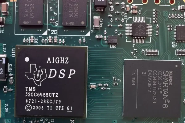
BGA failures can pass visual inspection and still fail in the field
BGA and FPGA packages hide every solder joint under the component body. Without X-Ray, DFM review, and test access planning, opens, bridges, voiding, head-in-pillow defects, and warpage problems can stay invisible until product testing or deployment.
Before the first build
Package pitch, pad design, stencil apertures, via-in-pad, moisture sensitivity, and board stack-up are reviewed before assembly starts.
When a design changes
BGA removal, site cleaning, reballing, replacement, X-Ray verification, and failure review help protect expensive parts and prototype boards.
When probe access is limited
High pin-count FPGAs often need JTAG access, boundary-scan planning, thermal review, boot memory programming, and functional test coverage.
Before shipment
First article inspection, X-Ray records, batch traceability, firmware revision control, and pass/fail logs can be aligned to your documentation needs.
Can your BGA or FPGA board be built and verified?
Check the package type, pitch, inspection scope, rework path, and test linkage before your build moves into production.
| Area | ACE support | Why it matters |
|---|---|---|
| Package types | BGA, FBGA, uBGA, LGA, QFN, CSP, PoP, large FPGA packages | Different package bodies need different stencil, placement, and thermal profiles. |
| Pitch range | 0.4 mm typical fine pitch; smaller packages reviewed case by case | Fine pitch increases bridge, open, solder volume, and pad design sensitivity. |
| Inspection | X-Ray inspection for hidden joints, AOI for surrounding components, FAI for new builds | BGA solder joints are invisible after placement and must be verified indirectly. |
| Void criteria | Project-specific acceptance aligned before production; IPC Class 2 or Class 3 on request | Thermal pads, power devices, and high-reliability products need clear acceptance rules. |
| Rework | BGA removal, pad cleaning, reballing, replacement, and X-Ray verification | Useful for prototype changes, expensive FPGA packages, and controlled failure recovery. |
| Testing linkage | JTAG, boundary-scan planning, firmware programming, custom FCT support | X-Ray confirms joints; electrical tests confirm connectivity and system behavior. |
Plan FPGA programming and test access before assembly
FPGA PCBAs often combine fine-pitch BGA soldering, high-speed routing, boot memory, power sequencing, thermal constraints, and limited physical probe access. We connect the assembly route to programming and test requirements before the build reaches production.
Confirm JTAG and boundary-scan access
Check test headers, chain access, net coverage, and devices that need in-system programming.
Reduce thermal and warpage risk
Check large package body size, PCB thickness, copper balance, reflow profile risk, and heat-sensitive areas.
Link programming to test records
Link firmware revision, boot memory, serial number, checksum, and functional test result to the production lot.
Send these details for a more accurate review
Gerber, BOM, pick-and-place data, assembly drawings, FPGA programming notes, test expectations, keep-out zones, and thermal requirements help us flag assembly risk earlier.
Know what happened under the package before boards ship
X-Ray inspection helps identify soldering defects under BGA, QFN, LGA, and PoP packages before boards leave the factory. For higher-risk builds, it is paired with process controls and electrical testing.
Voids
Air pockets inside solder joints can reduce mechanical strength and thermal transfer. Acceptance should be defined by package function and reliability class.
Bridges
Fine-pitch pads can short when solder volume, placement, or reflow conditions are not controlled tightly enough.
Opens
Open joints may be caused by insufficient solder wetting, pad contamination, component coplanarity, or board/package warpage.
Head-in-pillow
A high-risk intermittent defect where the solder ball and paste touch but do not fully merge during reflow.
Inspection evidence you can request
Catch BGA layout risks before they become soldering defects
A focused DFM review can prevent expensive BGA failures. These are the items our engineers check before quoting, stencil design, reflow setup, and first article approval.
MSL handling and baking
Confirm moisture sensitivity level, storage condition, baking need, and floor life before reflow.
Pad and solder mask design
Review NSMD/SMD pad strategy, solder mask registration, and pad geometry against package recommendations.
Via-in-pad control
Define filled, capped, or plugged vias to avoid solder wicking and hidden opens under the package.
Stencil aperture strategy
Tune solder paste volume for fine-pitch BGAs, QFNs, thermal pads, and mixed component densities.
Warpage and reflow profile
Check board thickness, copper balance, large package body risk, peak temperature, soak time, and cooling slope.
Underfill and coating needs
Decide whether underfill, conformal coating, or parylene coating is required before final assembly flow is locked.
Rework soldering expensive BGA and FPGA parts
Rework needs controlled heating, optical alignment, site preparation, component handling, and post-rework inspection. The goal is to recover value without creating pad damage or repeat failures.
Review
Confirm reason for rework, package type, board condition, and risk level.
Remove
Use controlled heating to remove the BGA while protecting nearby components.
Clean site
Clean pads, inspect solder mask, and prepare the site for replacement.
Reball or replace
Reball suitable components or place new components with optical alignment.
Verify
Run X-Ray inspection and agreed electrical or functional tests after rework.
What controlled BGA assembly looks like in practice
High-density FPGA controller
Multi-layer PCBA with fine-pitch FPGA, boot memory, dense passives, and high-speed interfaces. The build flow combined DFM review, controlled reflow, X-Ray inspection, and functional test planning.
Risk controlled
Warpage, hidden solder opens, firmware version control, and test access.

Documented BGA inspection package
High-reliability controller requiring documented inspection, batch traceability, and a defined pass/fail route before shipment to the customer.
Evidence delivered
X-Ray images, first article record, lot route, and agreed functional checks.
BGA & FPGA Assembly FAQs
Q
What files do you need to quote a BGA or FPGA assembly project?
What files do you need to quote a BGA or FPGA assembly project?
Please send Gerber files, BOM, pick-and-place data, assembly drawings, board stack-up if available, programming notes, and inspection or test requirements. For FPGA boards, include JTAG, boot memory, and firmware handling notes where relevant.
Q
Do you inspect every BGA with X-Ray?
Do you inspect every BGA with X-Ray?
For BGA, FPGA, QFN, LGA, and other hidden-joint packages, X-Ray inspection is used to verify solder quality in locations that cannot be checked visually. The exact inspection scope and evidence package can be aligned before production.
Q
Can you support BGA rework and reballing?
Can you support BGA rework and reballing?
Yes. Depending on board condition and component status, we can support BGA removal, site cleaning, reballing, replacement, and X-Ray verification. Rework feasibility is reviewed case by case because pad damage, thermal history, and component MSL status affect risk.
Q
How do you reduce head-in-pillow and open-joint risk?
How do you reduce head-in-pillow and open-joint risk?
We review paste volume, stencil aperture design, package coplanarity, MSL handling, board warpage, reflow profile, and pad design before production. For new or high-risk builds, first article inspection and X-Ray review are used before release.
Q
Do FPGA boards need boundary-scan testing?
Do FPGA boards need boundary-scan testing?
Not every FPGA board needs boundary scan, but it is very useful when dense BGA packages limit physical probe access. If your design exposes JTAG and supports boundary-scan coverage, it can help verify interconnects and support in-system programming.
Q
Can BGA assembly be combined with conformal coating or parylene coating?
Can BGA assembly be combined with conformal coating or parylene coating?
Yes, but coating and underfill decisions should be made early. Some connectors, test pads, RF areas, and programmed interfaces may need keep-out control. We can align assembly, inspection, test, and coating in one production route.
Related Services for BGA & FPGA Projects
BGA and FPGA assembly often depends on upstream SMT controls and downstream programming, testing, and protection.
SMT Assembly
Controlled stencil printing, placement, reflow, AOI, X-Ray, and first article approval for fine-pitch packages.
View SMT AssemblyIC Programming & Testing
Firmware flashing, JTAG support, boundary-scan planning, functional fixtures, serialized logs, and pass/fail reporting.
Explore Testing ServicesCoating & Protection
Conformal coating and in-house parylene coating options for high-density PCBAs used in harsh environments.
Review Coating OptionsNeed one team to manage the full BGA build route?
Explore PCBA Contract ManufacturingStart Your Projects Manufacturing Today!
Whether you need a quick quote or technical consultation, we're here to help.
Quick Response via WhatsApp
Get instant answers to your questions
Connect directly with our technical team for immediate assistance.
We typically respond within 30 minutes during business hours.
Business Hours: Mon-Fri 9:00-18:00 (GMT+8)