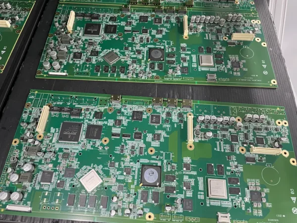
High-Precision SMT Assembly for Complex PCBs
From 01005 Passives to Large BGAs.
Trusted by European & North American OEMs for 15+ years.
Technical
Capabilities
Whether you need a quick prototype run or a stable low / large volume production batch.
- Lead-Free / RoHS Compliant
- IATF16949 Automotive Certification
- IPC-A-610 Class 2 & 3
| Capability | ACE SMT Specification | Why It Matters |
|---|---|---|
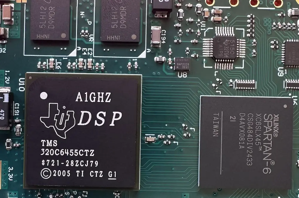
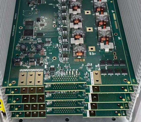
| Component Size | 01005, 0201, 0402, fine-pitch ICs, QFN, LGA, DFN, BGA and connectors | Supports high-density boards without moving fine-pitch work to another supplier. |
| Fine-Pitch / BGA | 0.3 mm fine-pitch connectors; BGA/QFN inspection with X-Ray for hidden joints | Reduces risk on hidden solder joints, bridges, opens and voiding. |
| Placement Accuracy | ±0.035 mm for chips; ±0.025 mm for QFP-class packages | Important for dense layouts, small passives and fine-pitch IC alignment. |
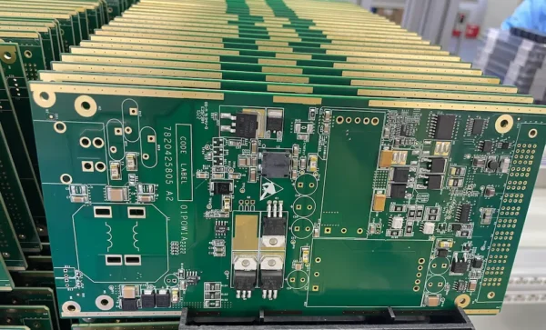
| PCB Types | Rigid PCB, flex PCB, rigid-flex PCB and aluminum / metal-core PCB | Useful for customers who need SMT plus PCB fabrication under one roof. |
| Reflow Process | 10-zone reflow oven; nitrogen reflow option; lead-free SAC305 process | Improves wetting control for lead-free, fine-pitch and oxidation-sensitive assemblies. |
| Inspection Gates | 3D SPI, online AOI, X-Ray for BGA/QFN, FAI and IPQC patrol | Catches print, placement and soldering defects before shipment. |
| Production Range | Prototype, NPI pilot run, low-volume and repeat production | Lets customers start small and scale without changing the process owner. |
| Compliance | RoHS lead-free process; IPC-A-610 Class 2 / Class 3 workmanship target | Matches industrial, automotive and high-reliability PCBA requirements. |
| Monthly Capacity | 52 million placements | Shows capacity for repeat production after prototype validation. |


SMT Manufacturing Process
A controlled SMT line is more than placement speed. We check files, materials, paste volume, component alignment, reflow profile and inspection data before your boards move to the next step.
File & Material Review
Gerber, BOM, pick-and-place data, polarity marks, package information and incoming components are checked before line setup.
Solder Paste Printing
Nano-coated stencil options, controlled squeegee settings and paste handling help stabilize fine-pitch solder deposition.
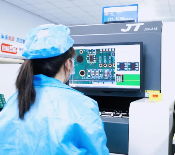
3D SPI
Solder paste volume, height, area and offset are inspected before placement, so print defects are corrected early.
Pick-and-Place
Vision-guided placement handles 01005 / 0201 passives, QFN, LGA, BGA and fine-pitch connectors with verified orientation.
Nitrogen Reflow
10-zone reflow profiles are tuned for board thickness, thermal mass and solder alloy to reduce tombstoning, opens and voiding.
AOI, X-Ray & FAI Release
AOI checks visible placement and solder defects. X-Ray verifies hidden BGA/QFN joints. First article approval is completed before repeat production.
We Don't Guess. We Verify.
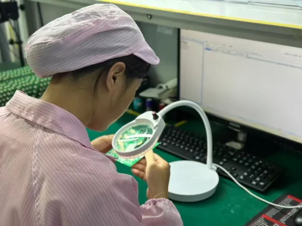
Online AOI
Detects missing components & polarity immediately after reflow.

X-Ray Inspection
For BGA & QFN. We verify voiding < 25% (IPC Class 3) and check for bridges.
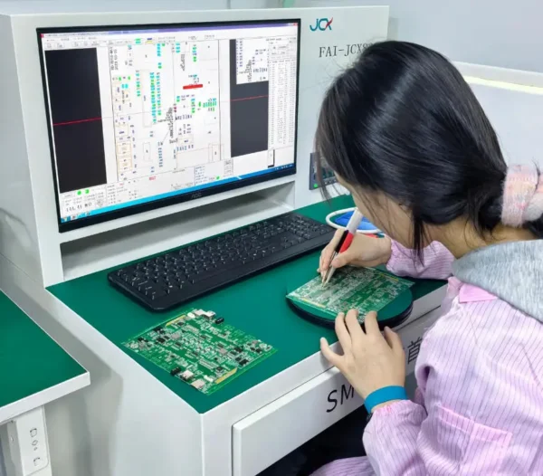
First Article Inspection (FAI)
Automated LCR measurement against BOM. Mass production starts only after 100% Pass.
IPQC Patrol
Regular line monitoring for ESD compliance, soldering temp, and operator standards.
SMT DFM Tips That Reduce Rework
Small layout decisions can change SMT yield, rework cost and lead time. Send your Gerber, BOM and pick-and-place files early so our engineers can check assembly risks before production.
Fiducials & Panelization
Add global fiducials and panel rails when possible. Keep enough clearance around rails, tooling holes and board edges for automated placement and depaneling.
BGA / QFN Land Pattern
For BGA and QFN packages, review pad size, solder mask opening, thermal pad design and via-in-pad filling to reduce voiding and solder wicking.
Stencil Aperture Strategy
Fine-pitch ICs, QFNs and small passives may need aperture reduction, windowpane openings or stepped stencil areas to stabilize paste volume.
Component Spacing
Leave enough spacing for pick-and-place nozzles, AOI visibility and rework. Dense layouts can be built, but they should be reviewed before release.
Polarity & Orientation
Clear polarity marks, pin-1 indicators and consistent component orientation reduce setup errors and speed up first article inspection.
Files for Fast Review
Send Gerber files, BOM with MPNs, pick-and-place data, assembly drawings and special test or programming notes for a faster SMT quote.
From First Article to Repeat SMT Production
We use the first build to verify files, process parameters and inspection criteria, then carry the approved setup into pilot and repeat production.
Prototype & DFM Review
We review BOM, Gerber, centroid and assembly drawings, then flag package, polarity, stencil, panel and test-point risks before SMT starts.
Pilot Run & Yield Feedback
First article inspection, SPI/AOI feedback and X-Ray review help confirm whether the SMT process is stable enough for repeat production.
ECO & Repeat Production
Approved changes are controlled by revision, BOM update and process notes so future SMT batches stay consistent with the validated build.
Trusted by Industrial
Automation Leaders.
We specialize in mission-critical electronics where failure is not an option. Our process controls are rigorous enough for automotive and medical standards.
Defect Rate
On this 12-Layer project
Components
High density placement
SMT Assembly FAQs
Q
What is the smallest component size you can assemble?
What is the smallest component size you can assemble?
We handle 01005 (0.4mm × 0.2mm) chip components routinely, with placement accuracy of ±0.035mm. For high-volume production, we recommend 0201 or larger for better yields and lower costs. 01005 requires specialized stencil design and nitrogen reflow profiles.
Q
How do you ensure BGA soldering quality?
How do you ensure BGA soldering quality?
We use 3D X-Ray inspection to detect voids, bridges, and missing balls. Our process guarantees voiding <25% (IPC Class 3 standard). For 0.4mm pitch BGAs, we use microsection analysis and optimize stencil apertures to achieve 100% wetting.
Q
Do you support lead-free and RoHS compliance?
Do you support lead-free and RoHS compliance?
Yes. Our standard process uses SAC305 lead-free solder (Sn96.5/Ag3.0/Cu0.5) and all materials are RoHS 3 compliant. We provide Certificates of Compliance and material declarations for medical and automotive customers requiring full traceability.
Q
What is the typical lead time for prototypes vs. production?
What is the typical lead time for prototypes vs. production?
Prototypes: 3-5 days for 5-50 pieces (expedite available for 48h). Production: 2-3 weeks for 1,000+ units depending on component availability. We offer consignment options if you supply critical/long-lead components to shorten TAT.
Q
What files do you need for a quote?
What files do you need for a quote?
We need Gerber files (RS-274X), BOM (Excel/CSV) with manufacturer part numbers, and Pick-and-Place/Centroid data. For complex boards, assembly drawings help clarify polarity and orientation. We accept Altium, Eagle, and KiCad native files for DFM review.
Q
What inspection methods do you use during SMT?
What inspection methods do you use during SMT?
We implement 3D SPI (Solder Paste Inspection) after printing, Online AOI after placement, and X-Ray for hidden joints (BGAs/QFNs). First Article Inspection (FAI) is mandatory for all new products before mass production ramp-up.
Q
Can you review my PCB layout before SMT
assembly?
Can you review my PCB layout before SMT assembly?
Yes. We can review fiducials, panelization, BGA via-in-pad, stencil aperture risk, component spacing, polarity marks and test-point access before production. Early DFM review helps reduce rework and avoid first-article delays.
Q
How do you move from prototype SMT
assembly to production?
How do you move from prototype SMT assembly to production?
We use the prototype or pilot run to confirm DFM comments, first article inspection, SPI/AOI results, X-Ray criteria and any functional test requirements. Approved changes are controlled by revision and BOM update before repeat production.
Other Services Available At ACE Electronics
From PCB fabrication to fully assembled products. Streamline your supply chain with our integrated manufacturing services.
Component Sourcing
Global sourcing of active and passive components, connectors, and modules. Procurement with traceability, counterfeit avoidance, and long-term availability planning.
Explore Component SourcingParylene Coating
In-house CVD parylene coating for ultimate moisture and chemical protection. Ideal for medical devices and harsh environments.
Learn About Parylene CoatingBox Build Assembly
Complete electromechanical integration: enclosures, cable harnesses, PCB mounting, and functional testing to finished product.
View Box Build ServiceNeed a complete manufacturing partner?
Explore All Turnkey ServicesStart Your Projects Manufacturing Today!
Whether you need a quick quote or technical consultation, we're here to help.
Quick Response via WhatsApp
Get instant answers to your questions
Connect directly with our technical team for immediate assistance.
We typically respond within 30 minutes during business hours.
Business Hours: Mon-Fri 9:00-18:00 (GMT+8)