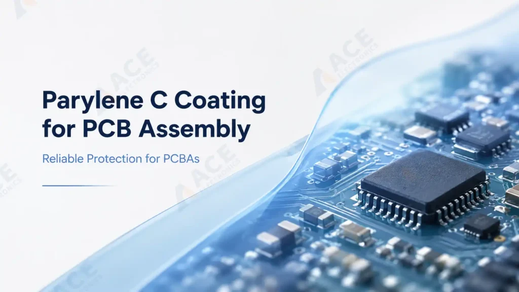
Parylene C coating is a vapor-deposited conformal coating widely used on PCB assemblies and electronics because it combines a strong moisture barrier, stable dielectric insulation, and very uniform thin-film coverage. Among the common Parylene grades, it is the one most often used for general electronics protection, especially when a product needs coverage on edges, leads, narrow gaps, and other hard-to-reach surfaces.
What Is Parylene C Coating?
Parylene C is one member of the Parylene family of polymer coatings. In PCB assembly, it is used as a very thin protective film deposited from vapor rather than sprayed, brushed, or dipped as a liquid. That deposition method is a major reason it is used on dense or complex electronics where liquid-applied coatings may leave thicker edge buildup or uneven coverage.
Within the Parylene family, type C is the grade most readers will see first in electronics work.
If you want a broader overview of how this material fits into the larger category, see the Parylene conformal coating guide. For a general comparison between vapor-deposited and liquid-applied coating methods, see the conformal coating process guide.
Why Parylene C Is the Widely Used for Electronics
'Parylene C' is the most common Parylene grade for electronics. It balances moisture blocking, electrical insulation, and cost for the majority of electronics projects.
Moisture Barrier
Humidity and condensation corrode exposed copper and solder joints over time. Parylene C stops moisture at just a few microns thick. On dense boards with fine-pitch parts and tight clearances, that thin profile is the point. It also insulates electrically without the weight and thickness of liquid coatings or potting.
Lower Cost Than Specialty Grades
Parylene N has lower dielectric loss. Parylene HT survives higher temperatures. Most PCBA projects do not need either. If your electronics products run at standard temperatures and does not push RF loss limits, Parylene C is the cheaper option. That is why it is the first grade most electronics would be considered.
If your board is RF-sensitive rather than general-purpose, compare this grade with our Parylene N coating guide before finalizing the coating choice.
Better Supply Chain Support
Every Parylene coating factory knows how to apply Parylene C. The material is in stock, the recipe is proven, and the quote is quick.
Parylene N and Parylene HT are different. Fewer shops keep the dimer on hand. You will wait longer for material and pay for extra process setup before production starts.
Fits for most of Electronics Projects
Industrial controls, automotive sensors, medical devices, and compact consumer electronics — Parylene C handles all of them because most of these products need long-term moisture protection, not extreme dielectric or thermal performance.
Key Parylene C Properties for PCB Assembly
| Property | Typical Value | What It Means for PCBA | |
|---|---|---|---|
| Dielectric strength | 5,600 V/mil (~220 kV/mm at 25 µm) | Thin film still insulates well. Good for dense boards and higher-voltage traces. | |
| Dielectric constant | 3.15 @ 60 Hz / 3.10 @ 1 kHz / 2.95 @ 1 MHz | Stable across common electronics frequencies. | |
| Water vapor transmission | 0.08 g·mm/(m²·day) | Low permeability = strong moisture barrier. | |
| Continuous service temp | 80 °C | Long-term safe limit for most industrial and consumer electronics. | |
| Short-term peak | 100–115 °C | Brief exposure only. Do not design to this number. | |
| Melting point | ~290 °C | Material ceiling. Operating temp stays far below this. | |
| Friction coefficient | 0.29 (static and dynamic) | Low-friction surface. | |
| Common thickness range | PCBA typically 5–20 µm | Thin enough for tight clearances and fine-pitch parts. |
Chemical Resistance
Parylene C resists most solvents, acids, bases, and industrial chemicals. Exact performance depends on concentration, exposure time, and what else is on the board. If your product faces a specific chemical environment, feel free to send inquiry to us for a targeted compatibility check.
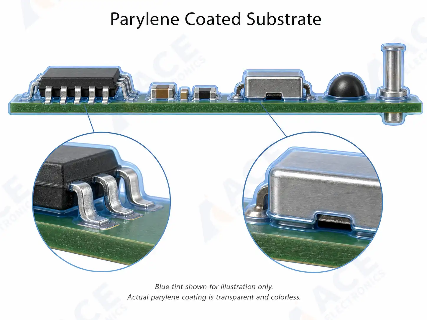
A thin Parylene C film can cover the PCB substrate and exposed features with very little added thickness.
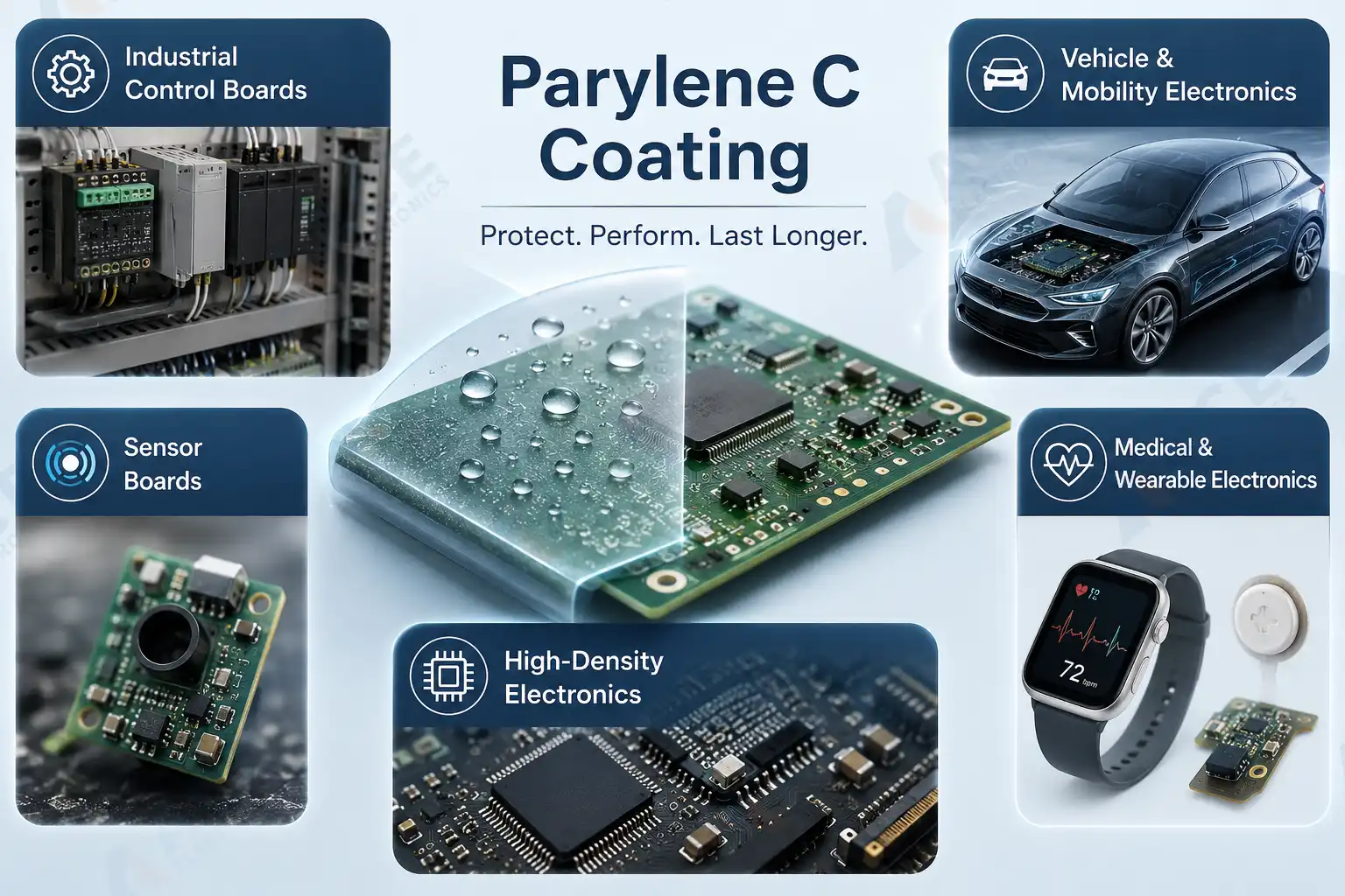
Common PCB Assembly Applications of Parylene C
| Application | Why Parylene C is commonly used |
|---|---|
| Industrial control boards | Helps protect exposed circuitry from humidity, corrosion, contamination, and long service life demands |
| Vehicle and mobility electronics | Thin conformal coverage is useful where boards may see condensation, dust, and repeated temperature cycling |
| Sensor boards | Uniform coverage supports compact assemblies with exposed fine features and small clearances |
| Medical and wearable electronics | A thin polymer film can be useful when space is limited and heavier protection methods are not desirable |
| High-density electronics | Very thin coverage helps when connector spacing, component height, and overall dimensional control matter |
Industrial control boards, sensor electronics, and other exposed assemblies are common applications where Parylene C is used for added protection.
Industrial control and mobility electronics are especially common contexts for this material. For example, ACE Electronics's Parylene-coated hydrogen forklift control board case study is a practical example of where a thin moisture-resistant coating can make sense on a control assembly that may face condensation and a harsher working environment.
A hydrogen forklift control board is a practical example of an industrial PCB assembly where Parylene coating may be selected for moisture and environmental protection.
Conclusion
Parylene C coating remains the most common electronics-grade Parylene because it combines moisture barrier performance, dielectric insulation, thin conformal coverage, and broad practical use across many PCB assembly projects in many industies.
If your projects need PCB Assembly and Parylene-coated, see ACE Electronics's Parylene coating service and PCB Assembly Service for production scope and manufacturing support.
Frequently Asked Questions
When is Parylene C a better choice than a liquid conformal coating?
When is Parylene C a better choice than a liquid conformal coating?
Parylene C is usually reviewed when a PCB assembly needs thinner and more uniform coverage than spray, brush, or dip coatings can easily provide. It is often considered for dense boards, exposed leads, narrow gaps, and products where moisture protection matters but extra coating buildup is not welcome.
What thickness is commonly specified for Parylene C on PCB assemblies?
What thickness is commonly specified for Parylene C on PCB assemblies?
Many PCB assembly uses fall in the 5 to 20 um range, although published ranges start lower and can extend much higher. The right thickness depends on the protection target, board geometry, electrical spacing, and any dimensional limits around connectors, housings, or mating parts.
What temperature range is realistic for Parylene C in electronics use?
What temperature range is realistic for Parylene C in electronics use?
For practical electronics use, 80 C is the common continuous-service reference point for Parylene C. Short-term published values are higher, often around 100 to 115 C, while melting point is about 290 C.
Can some areas of a PCB assembly be left uncoated?
Can some areas of a PCB assembly be left uncoated?
Yes. Connectors, test pads, grounding points, mating surfaces, and other functional areas are often defined as no-coat areas before production. That should be identified clearly in drawings, notes, or sample review, because Parylene will deposit on any exposed surface that is not protected.
What information should be prepared before asking for a Parylene C coating quote?
What information should be prepared before asking for a Parylene C coating quote?
The most useful items are the PCB assembly drawing or photos, the target coating area, no-coat areas, the expected thickness range, the product environment, and the order quantity or production stage. If you already know connector keep-out zones, mating surfaces, or test points that must stay open, include those early to reduce back-and-forth during quote review.