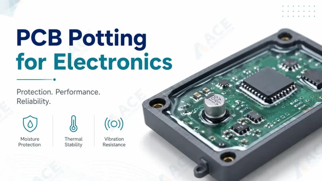
PCB potting is a protection process that fills a cavity or enclosure around an assembled PCB with a liquid compound—typically epoxy, polyurethane, or silicone. After curing, the compound forms a solid or gel barrier that seals the electronics against moisture, dust, vibration, and mechanical shock.
Potting is a form of encapsulation. Other encapsulation methods include dam and fill and glob top. This guide covers cavity-fill potting in the context of PCB assembly and final product integration.
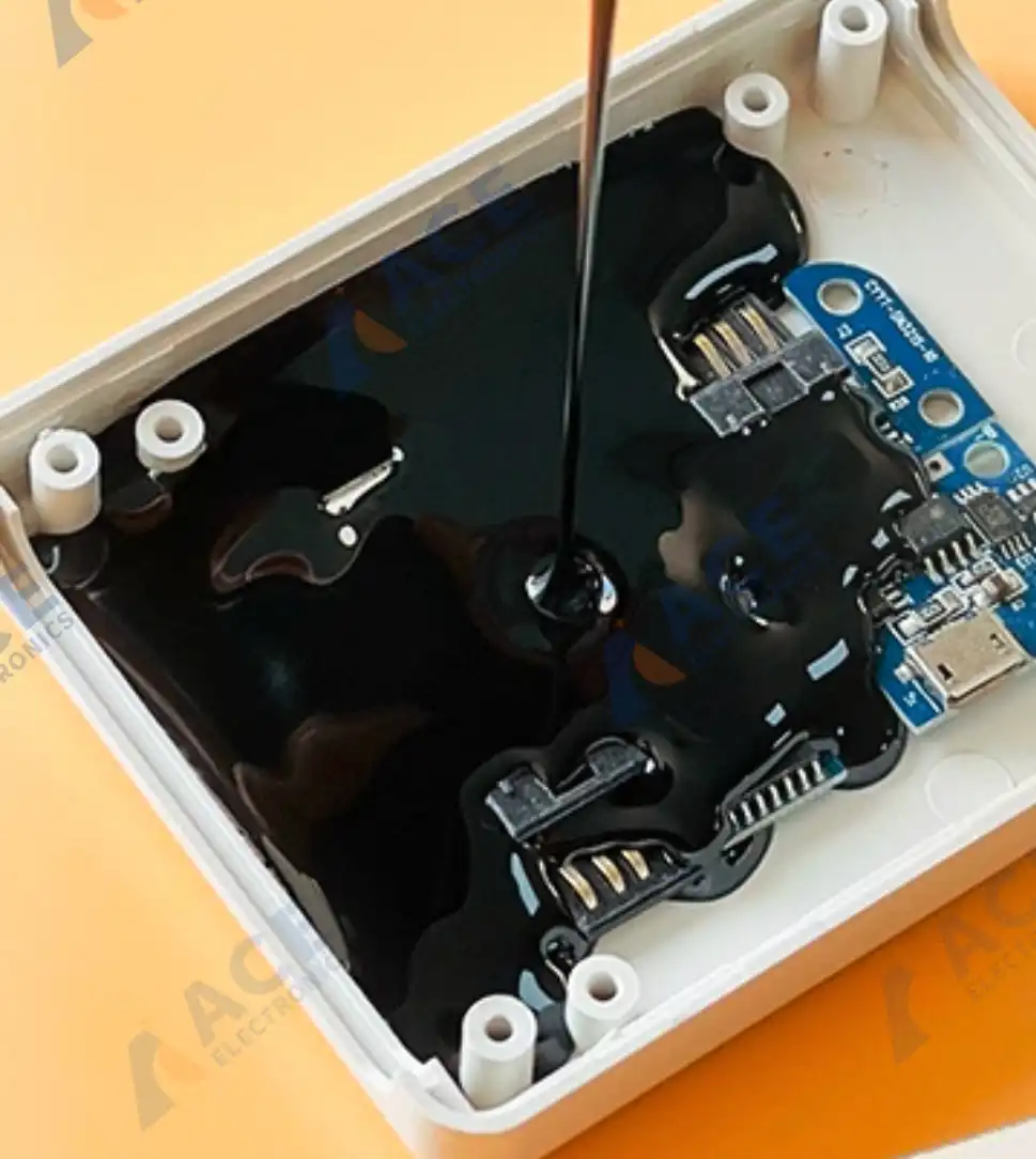
PCB potting fills the space around an assembled board with a cured compound for stronger environmental and mechanical protection.

A short overview of PCB potting in electronics production.
Why Assembled PCB Need to be Potted
Potting is used when conformal coating is not enough for protecting the PCBA. For example, the board faces conditions that demand thicker, full-volume protection:
Severe water and contamination
- Submersion, heavy spray, or high-pressure washdown
- Mud, abrasive dust, or chemical slurry that would breach a surface coating
Mechanical stress
- Constant vibration or shock that risks solder joint failure
- Structural support for tall or heavy components
Electrical isolation and safety
- High-voltage assemblies needing increased creepage and clearance
- Arc suppression in dense power electronics
Security
- Hiding circuit details, chips, and traces to prevent reverse engineering or tampering
Common PCB Potting Materials
| Material | Behavior | Typical applications | Key limitation |
|---|---|---|---|
| Epoxy | Hard, rigid, strong adhesion, high chemical resistance | Industrial controls, tamper-resistant assemblies, structural stability | Difficult to rework; can stress components during thermal cycling; tends to trap heat |
| Silicone | Soft, flexible, wide thermal range | Temperature-cycling environments, vibration-heavy products, delicate assemblies | Low structural rigidity; material may shift over time |
| Polyurethane | Balanced flexibility and durability | Moisture and abrasion exposure, general outdoor electronics | Rework remains difficult; formulation must match the use case |
Potting in PCB Assembly: When It Happens and Why
Potting only could be proceeded when the PCB is fully assembled, tested, and cleaned, but before final housing or product packaging.
Once the compound cures, you cannot access the components for repair or rework. Any soldering defect, failed test must be caught and fixed before the potting material goes on.
Typical Potting Sequence in Production
1. PCB Assembly Finishes
SMT placement, reflow, THT insertion, wave soldering, and any hand soldering are all done.
2. Inspection and Test Pass
AOI, X-ray, ICT, or functional test confirm the board works.
3. Board Cleaning and Drying
Flux residue, dust, or moisture trapped under the compound will cause corrosion or adhesion failure. The board need to be cleaned and fully dried before potting.
4. Enclosure or Cavity Preparation
The housing, mold, or dam structure is positioned.
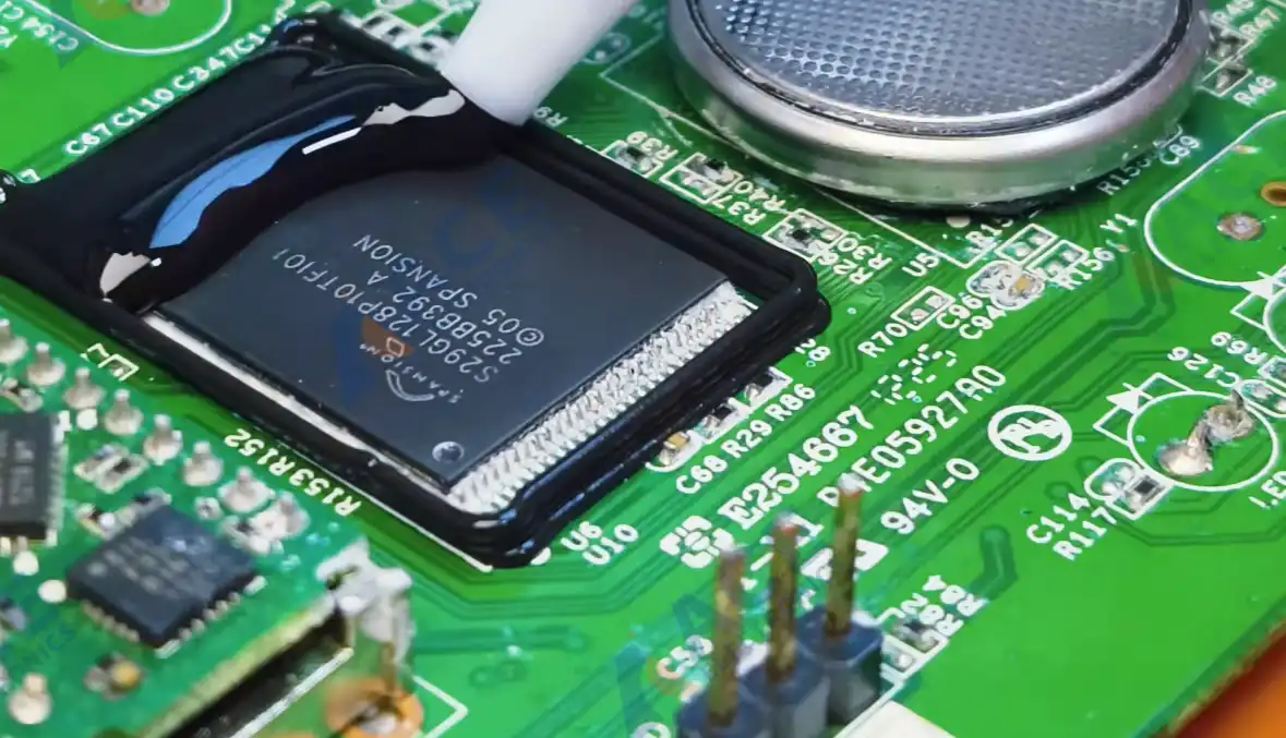
A dam-and-fill structure keeps the potting compound inside a defined area while leaving nearby connectors, components, or service zones open.
5. Compound Dispensing
The epoxy, polyurethane, or silicone compound is mixed, de-aired, and poured or dispensed into the cavity or the areas of PCBA.
6. Curing
The assembly cures at room temperature or in an oven, depending on the material. No handling until the compound reaches handling strength.
7. Final Assembly Continues
Labels, connectors, cables, housings, or packaging are added. The potted board is now treated as a sealed sub-assembly.
Design and Production Limits for Potting
Rework and Repair
Potting seals the board. Once the compound cures, you cannot swap a single component. If your product needs field repair, board replacement, or component-level troubleshooting, full potting is not suitable.
Heat Dissipation
Potting blocks or redirects heat. Some compounds help heat escape; others lock the heat in. If your board has power chips, regulators, or anything that runs hot, check the temperature before you decide what material and how much compound to use.
keep-out Areas
Connectors, switches, buttons, test points, and trim pots need a clear keep-out rule.
Enclosure Volume and Fill Control
Cavity depth, wall shape, vent paths, and compound volume all decide whether the fill covers evenly. Enclosure design and potting plan must be set together.
PCB Potting vs Conformal Coating vs Parylene
These three methods solve different protection problems.
| Method | Form | Thickness | Rework | Best fit |
|---|---|---|---|---|
| Conformal coating | Thin surface film | ~25–250 µm | Easier than potting | Dust, moisture, light chemical exposure, boards needing access |
| Parylene | Vapor-deposited polymer film | A few to tens of microns | Difficult | Dense boards, thin-film protection, geometry-sensitive assemblies |
| Potting | Resin mass around the assembly | Millimeters (cavity depth) | Hardest | Harsh environments, mechanical support, enclosure-level sealing, PCB layout Protection |
If you want a deeper explanation of how vapor-deposited thin-film protection differs from both liquid coating and full potting, see our Parylene conformal coating guide.
Potting surrounds the board with significantly more material than a conformal coating or Parylene film. The trade-offs:
- Stronger sealing
- Harder service access
- Higher weight and volume change
- Greater thermal impact
- Tighter enclosure coordination
Pre-Production Checklist
| Review point | Why it matters |
|---|---|
| Test sequence | Pot after test to avoid trapped faults |
| Compound family | Epoxy, silicone, and polyurethane differ in rigidity, thermal behavior, and rework access |
| Fill area | Connectors, vents, sensors, and light paths need defined keep-out zones |
| Enclosure design | Cavity geometry affects flow, air entrapment, and coverage uniformity |
| Thermal path | Heat-heavy boards may need a different compound or protection strategy |
| Rework policy | Define service expectations before selecting potting |
Coordinate the protection plan with PCB assembly services and final box build assembly early. Potting works best when designed into the full production route.
Frequently Asked Questions
What is PCB potting?
What is PCB potting?
PCB potting fills a cavity or enclosure around an assembled circuit board with a liquid compound that cures into a protective barrier.
What is the difference between potting and conformal coating?
What is the difference between potting and conformal coating?
Conformal coating adds a thin surface film (~25–250 µm). Potting fills the space around the assembly with a much thicker material mass. Potting provides stronger sealing and mechanical support; conformal coating preserves service access.
Is PCB potting the same as encapsulation?
Is PCB potting the same as encapsulation?
Potting is one form of encapsulation. Encapsulation is the broader term and also includes dam and fill and glob top.
What materials are commonly used for PCB potting?
What materials are commonly used for PCB potting?
Epoxy, silicone, and polyurethane. Each differs in rigidity, thermal behavior, vibration damping, and rework feasibility.
Why should a board be tested before potting?
Why should a board be tested before potting?
Cured resin blocks probe access and makes component replacement impractical. Testing must be completed before the compound is applied.