Parylene conformal coating is a vapor-deposited protective film used on PCB assemblies that need very uniform coverage, strong moisture protection, and consistent barrier performance on densely packed or complex boards. Unlike spray, brush, dip, or selective liquid coatings, Parylene is deposited via chemical vapor deposition (CVD) inside a vacuum chamber. Because the film forms from a gas-phase monomer, it wraps around edges, fills narrow gaps, and coats under components evenly — areas that liquid coatings often miss or leave with pinholes.
If you are reviewing coating options for a PCBA order, this article covers when Parylene fits, how the process differs from liquid coatings, and what drives thickness, cost, masking, rework, and lead time.
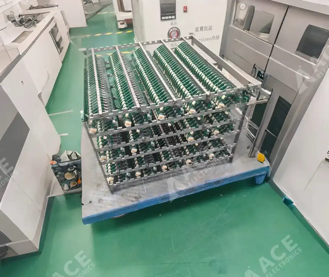
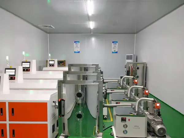
BLDC motor PCB assemblies mounted on suspension fixtures before entering the parylene vacuum chamber. Fixture spacing, masking, and loading layout affect coating uniformity and chamber throughput.
What Is Parylene Conformal Coating?
Parylene conformal coating is a thin polymer film applied to an assembled PCB through chemical vapor deposition. It is used when a board needs protection from moisture, condensation, corrosion, contamination, and electrical leakage, but liquid coatings cannot reach narrow gaps, sharp edges, and areas under densely packed components.
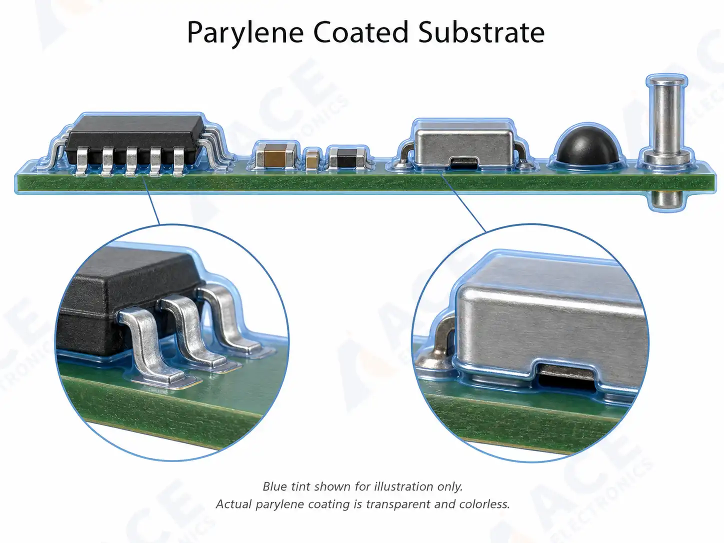
The core difference between normal conformal coating and Parylene, is the application method. Standard conformal coatings are usually applied as liquids. Parylene is deposited from vapor, the solid raw material — parylene dimer — is heated under vacuum, converted to a reactive monomer gas, and deposited onto every exposed surface inside the coating chamber. The result is an ultra-thin, pinhole-free film that conforms to the exact topography of the assembly.
Key characteristics of parylene conformal coating:
- Truly conformal: coats edges, corners, vertical surfaces, and tight gaps evenly — not possible with most liquid coatings
- Ultra-thin: effective protection can be achieved at 5 to 25 microns, keeping added mass and dimensional change low
- Pinhole-free: the molecular-level deposition leaves no voids or thin spots
- Room-temperature process: no thermal stress on solder joints or sensitive components during application
- No solvents or curing: the entire process is dry; there is no outgassing and no liquid phase
These characteristics make parylene a practical choice for densely assembly PCB and electronics products that must survive harsh environments without failure.
Parylene forms a thin, continuous polymer film over the PCB substrate and exposed features, which helps explain its strong barrier performance at low thickness.
For a broader comparison of coating materials and general PCB assembly protection options, see ACE Electronics' conformal coating guide for PCB assembly.
What Does Parylene Coating Protect PCB Assemblies From?
Parylene conformal coating is used to protect PCB assemblies from environmental, electrical, and chemical risks that can cause corrosion, leakage current, short circuits, intermittent failure, or long-term reliability problems.
For PCBA projects, the main protection targets include:
| Risk | How Parylene Helps |
|---|---|
| Moisture and condensation | Forms a continuous moisture barrier over exposed copper, solder joints, component leads, and PCB surfaces |
| Corrosion | Helps isolate metal surfaces from humidity, salt, contaminants, and corrosive gases |
| Electrical leakage | Provides high dielectric insulation between closely spaced conductors |
| Dust and contamination | Covers exposed surfaces and reduces the effect of conductive or ionic contamination |
| Chemical exposure | Resists many solvents, cleaning agents, acids, bases, and industrial fluids |
| Salt spray and harsh atmosphere | Helps protect boards used in outdoor, marine, automotive, and industrial environments |
| Tight gaps and component undersides | Vapor deposition allows coating to reach edges, crevices, and areas under components more reliably than liquid coatings |
This is why parylene is often considered for PCB assemblies used in motor control, automotive electronics, sensors, medical devices, aerospace electronics, industrial IoT, and other products where small amounts of moisture, corrosion, or electrical leakage can lead to failure.
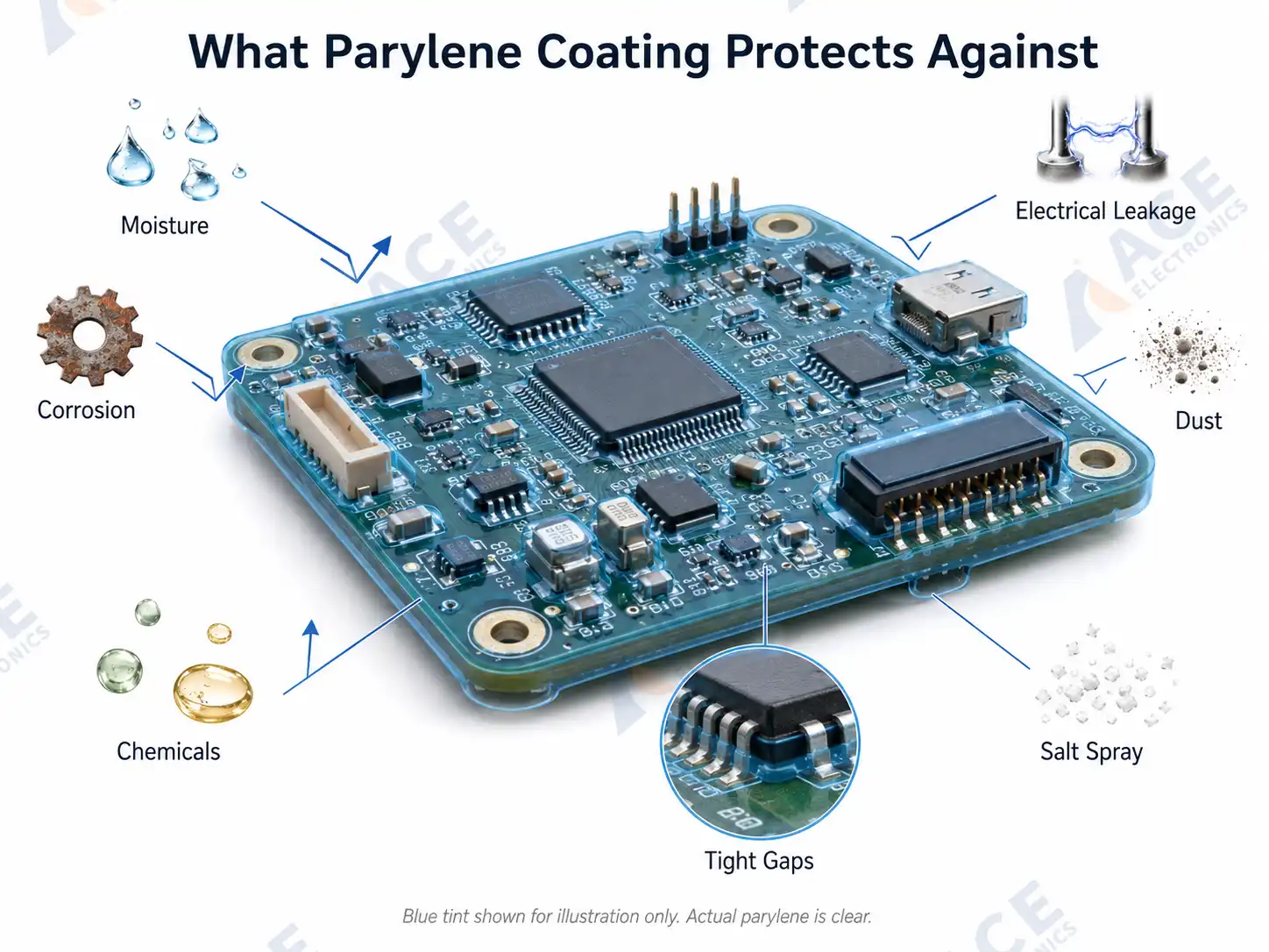
Parylene conformal coating forms a thin, uniform protective film over PCB assemblies to help protect exposed surfaces, component leads, solder joints, edges, and tight gaps from moisture, corrosion, electrical leakage, dust, chemicals, and salt spray.
How Parylene Coating Protects PCB Assemblies: Key Properties
The table below summarizes the values of the Parylene C that widely used.
| Property | Typical Parylene C Value | Why It Matters for PCBA |
|---|---|---|
| Dielectric strength | ~5,600 V/mil / 220 kV/mm at 25 µm | Provides high insulation in an ultra-thin film and helps improve protection between closely spaced conductors |
| Dielectric constant | ~3.10 at 1 kHz; published values are ~3.15 at 60 Hz and ~2.95 at 1 MHz | Supports predictable electrical behavior for many PCB insulation and signal-protection applications |
| Water vapor transmission / permeability | ~0.08 g·mm/(m²·day) | Provides a strong moisture barrier compared with many liquid conformal coatings |
| Continuous service temperature | Parylene C: up to 80°C continuous; Parylene HT: up to 350°C continuous | The operating temperature limit depends strongly on the selected Parylene grade |
| Coefficient of friction, static/dynamic | ~0.29 / ~0.29 | Dry-film lubricity can help with low-load sliding or contact interfaces |
| Coating thickness range | Typically ~0.5–50+ µm; many PCBA applications use ~5–20 µm | Thin enough for tight spaces while still providing electrical and environmental protection |
| Chemical resistance | Resistant to many organic solvents, acids, bases, and industrial fluids | Helps protect assemblies exposed to cleaning agents, chemicals, and harsh industrial atmospheres |
Moisture and Chemical Barrier
Parylene forms a thin, continuous barrier against moisture, salt spray, and many chemicals. For PCB assemblies, it helps protect exposed copper, solder joints, component leads, and sensitive circuits without the thickness or weight of potting or encapsulation.
Dielectric Insulation
Parylene provides strong electrical insulation at very low thicknesses, typically around 5–20 µm for many PCBA applications. This helps protect closely spaced conductors, reduce leakage risk, and improve insulation in high-voltage or high-density designs.
Conformality and Crevice Penetration
The vapor-phase deposition reaches areas that liquid coatings cannot reliably cover: under BGAs, between closely spaced pins, inside connector bodies, and across sharp board edges. This is one of the defining advantages of parylene conformal coating over spray or dip alternatives.
Types of Parylene Conformal Coating
| Parylene Type | Dielectric Constant / Dissipation Factor @ 1 kHz | Continuous Service Temp | Short-Term Temp Limit | Melting Point | Key Characteristics | Best For | Common PCBA Thickness Range |
|---|---|---|---|---|---|---|---|
| Parylene N | 2.65 / 0.0002 | 60°C | 80–95°C | 420°C | Low dielectric constant, very low dissipation factor, strong crevice penetration | RF or low-loss dielectric applications, tight-cavity assemblies, low-friction surfaces | 1–10 µm |
| Parylene C | 3.10 / 0.019 | 80°C | 100–115°C | 290°C | Excellent moisture barrier, good dielectric strength, widely available | General PCBA protection, sensors, medical electronics, industrial assemblies | 5–20 µm |
| Parylene D | ~2.8 / ~0.003 | 100°C | 120–135°C | 380°C | Higher temperature capability than C, good chemical and gas barrier performance | Industrial electronics needing higher temperature capability than C | 5–20 µm |
| Parylene F | ~2.1–2.5 / ~0.001–0.02 | 200°C | 250°C | Not commonly specified | Better thermal and UV resistance than N/C, low-loss fluorinated chemistry | High-temperature electronics, UV-exposed assemblies, selected medical devices after validation | 5–20 µm |
| Parylene HT | 2.20 / 0.0020 | 350°C | 450°C | >500°C | Highest thermal stability, strong UV resistance, fluorinated chemistry | Aerospace, downhole electronics, under-hood automotive sensors, high-temperature assemblies | 5–15 µm |
Temperature values based on industry literature for long-term (≈10+ years) and short-term (≈1 month) exposure in oxygen-containing atmospheres. In inert (oxygen-free) environments, the operational range extends significantly — from as low as −270 °C to as high as 450 °C, depending on type.
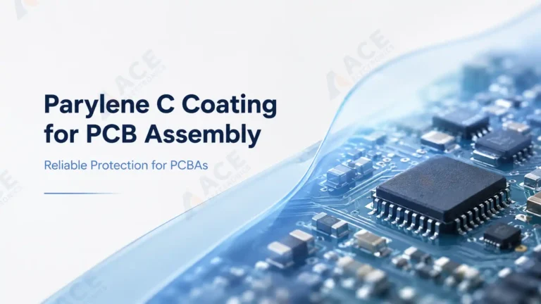
Parylene C — The Workhorse
If you are choosing between Parylene variants, start with type C. It is the most widely used grade for electronics protection. It blocks moisture well, insulates electrically, and deposits faster than N or D. That shorter chamber time keeps the cost down. If your team is evaluating Parylene for the first time, C is the practical starting point.
If your project is closer to general-purpose moisture protection than RF tuning or specialty thermal demands, see our Parylene C coating for PCB assembly guide for a more focused review of where this grade fits.
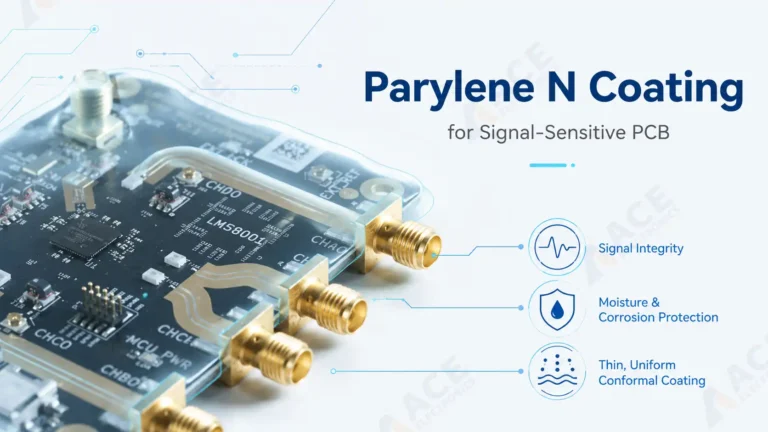
Parylene N — For RF and High-Frequency Applications
Parylene N offers the lowest dielectric constant and dissipation factor among the parylene family. It is the preferred choice when signal integrity matters — for example, on RF modules, antenna boards, and high-speed digital assemblies where coating-induced losses must be minimized.
If the PCB assembly is RF-sensitive, antenna-related, or otherwise sensitive to dielectric loading, review our Parylene N coating guide for a more specific discussion of electrical performance and use cases.
Parylene F and HT — For Extreme Environments
Parylene F provides higher temperature resistance and improved UV stability compared to Parylene C. Parylene HT extends the operating range further, to approximately 350 °C continuous. These types are specified when the assembly must survive autoclave cycles, engine-compartment temperatures, or long-term outdoor UV exposure.
For production runs that need high-temperature parylene options or low-loss parylene types for RF-sensitive areas, ACE Electronics supports multiple parylene formulations and can help align the material choice with your operating environment. Learn about our in-house parylene coating services.
How the Parylene Coating Process Works
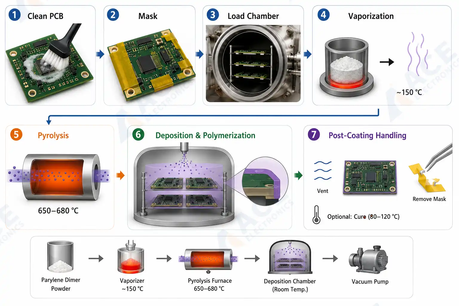
The parylene coating workflow starts with clean, dry assemblies and keep-out definition, then moves through vapor deposition, de-masking, thickness verification, and inspection.
The Parylene coating process starts with a clean, dry PCB assembly. Flux residue, particles, oils, or trapped moisture can affect coating quality, so board condition before coating matters.
Unlike acrylic, silicone, or urethane conformal coatings, Parylene is vapor-deposited rather than sprayed, brushed, or dipped as a liquid. That vapor-phase process is why it can coat edges, leads, narrow gaps, and other complex surfaces more evenly.
Masking and inspection are still important parts of the process. Connectors, test pads, grounding points, and other no-coat areas may need to stay open, and finished assemblies are typically checked for coating coverage and thickness.

This factory video shows PCB assemblies being masked, suspended on coating fixtures, and prepared for parylene deposition in the vacuum chamber.
Parylene Coating Thickness
Specify thickness when you request the quote. It controls fit, insulation, sealing, and cost.
Typical Range
Parylene runs 2–25 µm. Liquid coatings run 25–100 µm. Vapor deposition creates a dense film, so Parylene achieves the same protection with less bulk.
What Sets the Number
| Factor | Practical Rule |
|---|---|
| Mechanical clearance | < 0.1 mm gap → 2–5 µm |
| Harsh environment | Salt spray, condensation → 10–25 µm |
| Electrical load | High voltage → thicker film or different grade |
| Parylene grade | C, N, D, F have different deposition rates and barrier density |
| Customer spec | Some programs lock a range (e.g., 8–13 µm) and require coupon proof |
The Risk at Both Ends
Too thin: gaps, pinholes, failed barrier. Too thick: fit issues, masking residue, longer cycle time, higher cost.
Match the thickness to your project's real constraint.
What Affects Parylene Coating Cost?
Material is the smallest part of the bill. Most of the cost is time in the chamber, labor on the bench, and engineering before production starts.
Cost Drivers
Coated area. Larger boards use more dimer powder and occupy more fixture space. That extends the cycle.
Thickness target. Every extra micron adds chamber time. A 13 µm film takes roughly twice the cycle of a 5 µm film.
Masking complexity. Each connector, test point, LED window, or keep-out zone means hand work before and after deposition. Complex boards can spend more time masking than coating.
Batch size. The chamber has a fixed setup cost per run. Ten boards or one hundred boards pay the same setup. Small batches spread that cost over fewer units.
Cleaning and prep. Heavy flux residue or moisture requires extra bake and clean steps before the board can enter vacuum.
Inspection level. Thickness verification, adhesion testing, photo records, and customer-specific reports add lab time after deposition.
The Real Point
For Parylene, masking labor and batch efficiency usually drive the price more than the raw material.
When you send an RFQ, include:
- board dimensions and coated area
- thickness target or spec range
- a photo or drawing with keep-out zones marked
- annual volume and expected lot size
- any inspection or documentation requirements
Without these details, the quote is a guess.
Parylene coating cost and lead time depend on chamber loading, masking complexity, thickness target, and inspection requirements as much as on coating material.
Parylene vs. Liquid Conformal Coatings
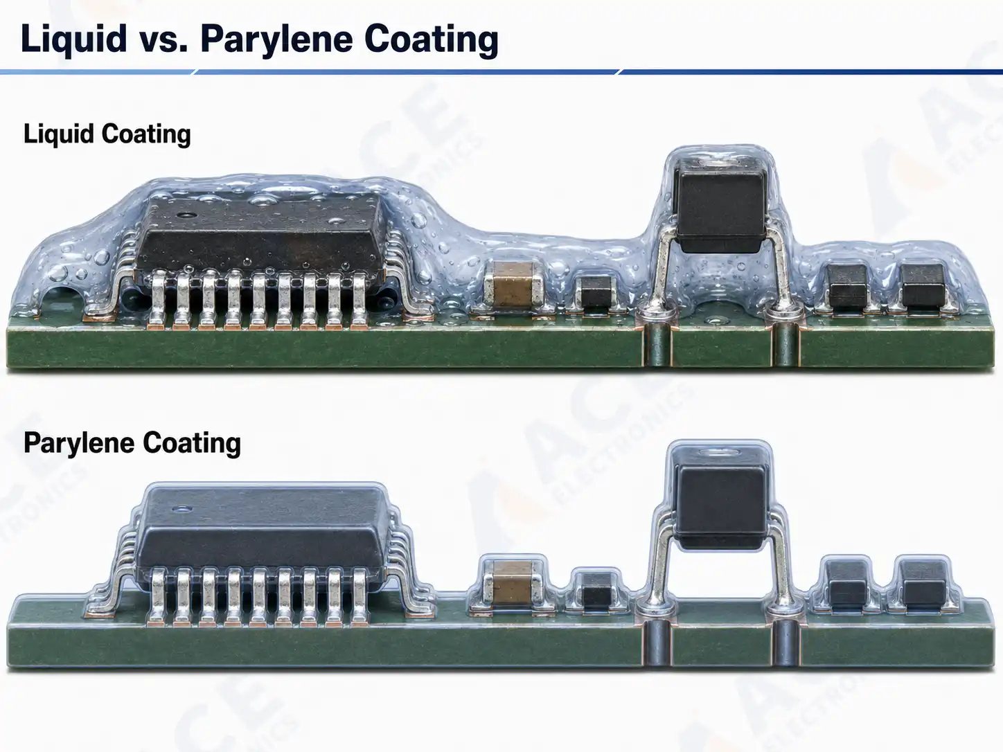
Liquid conformal coatings and parylene protect PCB assemblies in different ways. The application method changes film thickness, edge coverage, hidden-area coverage, and rework planning.
When choosing a protection strategy, the comparison between parylene conformal coating and liquid conformal coatings (acrylic, silicone, polyurethane) comes up frequently. The table below highlights the practical differences that matter for PCB assembly.
| Criteria | Parylene Conformal Coating | Acrylic (AR) | Silicone (SR) | Polyurethane (UR) |
|---|---|---|---|---|
| Application method | CVD (vacuum, vapor phase) | Spray, dip, or brush | Spray, dip, or brush | Spray, dip, or brush |
| Minimum effective thickness | 2–25 µm | 25–75 µm | 50–200 µm | 25–75 µm |
| Coverage under components | Excellent (vapor penetration) | Limited (capillary action only) | Limited | Limited |
| Edge coverage | Uniform, no thinning | Thinner at edges, pooling in corners | Thinner at edges | Thinner at edges |
| Reworkability | Difficult (mechanical removal) | Easy (solvent strip) | Moderate to difficult | Difficult |
| Moisture barrier per micron | Superior | Good | Good | Good |
| Chemical resistance | Excellent | Moderate | Good | Excellent |
| Thermal range | −200 °C to +350 °C (different type) | −65 °C to +125 °C | −55 °C to +200 °C | −65 °C to +125 °C |
| Batch processing time | Hours (vacuum cycle) | Minutes to hours | Minutes to hours | Minutes to hours |
| Relative cost | Higher | Lower | Moderate | Moderate |
Still deciding between acrylic, silicone, and urethane? Start with our conformal coating for PCB assembly guide overview.
When to Choose Parylene for Your PCBA Project
Before you request parylene coating, first check whether the board actually needs this level of protection.
Parylene is often worth reviewing in these situations:
- Fine-pitch SMT and dense layouts. Vapor deposition can cover narrow gaps, sharp edges, and areas under tightly spaced components more evenly than many liquid coatings.
- Humidity, condensation, or corrosive air. Parylene forms a strong moisture and chemical barrier for boards exposed to salt spray, industrial vapors, or long-term condensation risk.
- Long service life. It is often specified for products expected to run for years in industrial, automotive, energy, medical, or outdoor environments.
- Tight mechanical clearance. Parylene usually adds much less thickness than liquid conformal coatings, which helps when the board fits into a narrow enclosure or near contact surfaces.
- High cost of failure. It is commonly reviewed when field repair, replacement, or downtime would be expensive.
Parylene is usually not the first choice when the product only faces a clean indoor environment and easier rework matters more than maximum coverage. It requires vacuum deposition, clear masking strategy, and a defined repair plan before production starts.
Applications by Industry
| Industry | Typical Parylene Application | Why Parylene Is Selected |
|---|---|---|
| Medical devices | Implantables, wearables, diagnostic probes | Biocompatibility, ultra-thin profile, reliable barrier protection |
| Automotive and industrial vehicles | ECUs, sensors, BMS control boards, forklift controllers | Moisture and corrosion resistance under thermal cycling. Read case study → |
| Aerospace and defense | Avionics, satellite electronics, UAV controls | Outgassing control, wide temperature range, high reliability |
| Industrial IoT | Outdoor sensors, connected field devices | Long-term humidity and contaminant protection |
| Consumer electronics | Hearables, wearables, waterproof handhelds | Thin-film moisture barrier without added bulk |
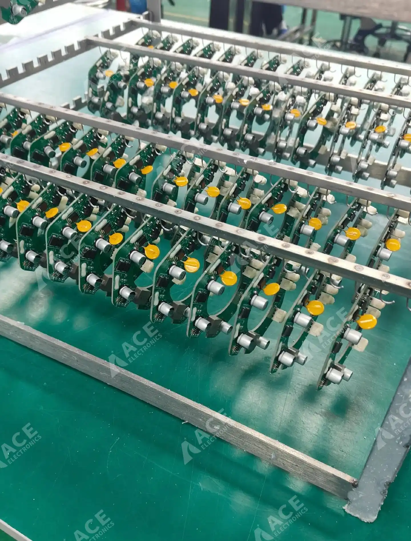
Close-up of BLDC motor PCB assemblies after cleaning, masking, and fixture loading, ready to enter the parylene deposition chamber.
Example: BLDC Motor Control PCB Assembly
A brushless DC motor control board is the kind of assembly where Parylene often makes practical sense, not just technical sense. The board is typically dense with SMT components, exposed leads, tall capacitors, and several multi-pin connectors. In operation, motor control environments can expose the board to humidity, vibration, dust, and condensation — conditions that liquid conformal coatings may not handle reliably over years of service.
Before this board entered the vacuum chamber, several decisions had to be made on the production floor:
- Connectors and test pads needed masking. Every exposed contact surface, programming header, and mating interface had to be sealed. On a connector-heavy board, masking can take longer than the coating cycle itself.
- Coating thickness was confirmed against the application. A thinner film would not hold up under condensation cycling; The target range was locked at 20um.
- Keep-out zones were defined and signed off. Any area that needed to remain uncoated — ground pads, heatsink interfaces, edge connectors — was marked on the masking map and verified after deposition.
- Fixture loading determined batch throughput. Spacing boards too tightly reduces coating uniformity; spacing them too far apart wastes chamber capacity. The loading layout was planned to balance cycle time and film quality.
Buyer Checklist: Evaluating Parylene for a PCBA Production Run
Use the following checklist when discussing parylene conformal coating with your assembly partner or coating specialist.
Operating Environment
- [ ] Will the assembly face sustained humidity, condensation, or salt spray?
- [ ] Will it be exposed to fuels, solvents, or industrial chemicals?
- [ ] What is the expected temperature range during operation and storage?
Board Geometry
- [ ] Does the board have fine-pitch components, BGAs, or tight clearances?
- [ ] Are there tall components, connectors, or mechanical interfaces that require masking?
- [ ] Are there sharp edges, vias, or crevices that could trap liquid coatings?
Electrical Requirements
- [ ] What dielectric strength is required between critical nets?
- [ ] Is signal integrity at high frequencies a concern?
- [ ] Are there high-voltage sections that need insulation at minimal thickness?
Production and Cost
- [ ] What is the expected annual volume: prototype, low-volume, or mass production?
- [ ] Is the production cadence compatible with batch vacuum processing?
- [ ] What is the estimated cost of a field failure compared with the added cost of parylene coating?
Quality and Acceptance
- [ ] What coating thickness range is specified?
- [ ] How will coating coverage and adhesion be verified?
- [ ] Are there IPC, MIL, FDA, or customer-defined standards the coating must meet??
If your PCB assembly project may need parylene conformal coating, send your board drawing, keep-out map, target thickness, environment notes, and production quantity early. We can review whether parylene fits the geometry, protection requirement, and delivery plan before quoting. For service scope, see ACE Electronics' Parylene coating service.
Frequently Asked Questions
When should I choose parylene instead of acrylic, silicone, or urethane coating?
When should I choose parylene instead of acrylic, silicone, or urethane coating?
Choose parylene when the PCB assembly has tight spacing, fine-pitch components, high humidity exposure, corrosion risk, or areas that liquid coatings may not cover reliably. If low cost and easy rework are the top priorities, acrylic, silicone, or urethane may be a better first option.
What information is needed to quote parylene coating for a PCB assembly?
What information is needed to quote parylene coating for a PCB assembly?
Useful information includes the PCB size, assembly drawings, coating thickness target, no-coat areas, connectors or test points that need masking, quantity, inspection requirements, and the operating environment. Photos of the assembled board are also helpful for checking masking difficulty.
What coating thickness should I specify for parylene on PCB assemblies?
What coating thickness should I specify for parylene on PCB assemblies?
Many PCBA projects use parylene in the 5–20 µm range, but the right thickness depends on voltage, environment, board geometry, parylene type, and reliability requirements. Very thin coatings may work for tight-clearance protection, while harsher environments or higher insulation needs may require a thicker film.
Is parylene coating suitable for high-voltage PCB assemblies?
Is parylene coating suitable for high-voltage PCB assemblies?
Yes. Parylene can be a strong option for high-voltage or high-density designs because it provides high dielectric strength at low thickness. The final decision should still consider working voltage, spacing, creepage and clearance, contamination level, coating thickness, and inspection criteria.
Can the PCB assembly be tested after parylene coating?
Can the PCB assembly be tested after parylene coating?
Yes, but the test plan should be reviewed before coating. Any test pads, programming connectors, calibration points, or contact areas needed after coating must be masked. If final testing requires electrical contact with coated areas, the process flow may need to be changed.