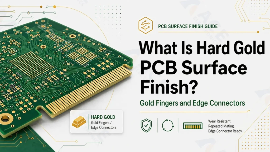
If your PCB has gold fingers, edge connectors, battery contacts, keypad contacts, or another repeated-contact area, hard gold may be the right surface finish.
The short answer: hard gold is a wear-resistant PCB surface finish used on contact areas that need repeated insertion, sliding, wiping, or probing. It is usually applied selectively, while the rest of the PCB uses a solderable finish such as ENIG, OSP, HASL, immersion silver, or ENEPIG.
Hard gold is different from ENIG. ENIG is mainly used for solderable pads, BGA, QFN, fine-pitch SMT, and general assembly reliability. Hard gold is mainly used where the PCB surface works as an electrical contact.
For a broader comparison of all common finishes, read our guide on how to choose PCB surface finish. This article focuses only on hard gold.
Quick Answer: What Is Hard Gold?
Hard gold is an electrolytic gold plating finish applied over a nickel barrier layer. The gold layer is harder and more wear-resistant than immersion gold, so it is used on PCB areas that need stable electrical contact after repeated mechanical use.
| Item | Simple explanation |
|---|---|
| Full name | Hard electrolytic gold plating over nickel |
| Surface type | Metallic, wear-resistant contact finish |
| Applied on | Gold fingers, edge connectors, contact pads, keypad contacts, test contacts |
| Main purpose | Provide durable electrical contact under repeated mechanical wear |
| Main advantage | High wear resistance and stable contact performance |
| Main limitation | Higher cost and not the usual choice for general solder pads |
| Best fit | Gold fingers, plug-in modules, field-replaceable boards, repeated-contact interfaces |
| Use with caution | Large solderable pads, cost-sensitive boards with no contact-wear requirement |
Hard gold is usually a selective finish. A PCB may use ENIG on SMT pads and hard gold only on the edge connector fingers. This gives the board solderability where components are assembled and wear resistance where the PCB mates with a connector.
How Hard Gold Works on a PCB
A hard gold finish is built as a plated metal stack over exposed copper.
The typical structure is:
| Layer | Role |
|---|---|
| Copper | Base conductive PCB feature |
| Nickel | Barrier layer between copper and gold |
| Hard gold | Wear-resistant contact surface |
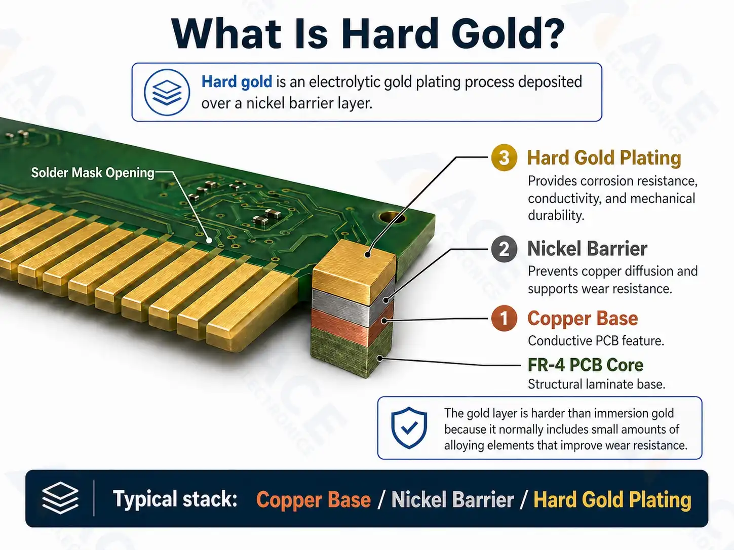 Figure 1. Typical hard gold layer stack-up on a PCB: copper base for conductivity, nickel barrier to prevent copper diffusion, and electrolytic hard gold plating for corrosion resistance and wear durability. Hard gold is selectively applied to high-wear areas such as edge connectors — not standard solder pads.
The nickel layer helps prevent copper diffusion and provides a hard base under the gold. The hard gold layer provides corrosion resistance, conductivity, and mechanical durability at the contact surface.
In most PCB projects, hard gold is not applied across the whole board. It is plated only on the defined contact area, such as card-edge fingers. The remaining solderable pads use another surface finish chosen for assembly.
A common finish combination is:
| Board area | Typical finish |
|---|---|
| SMT component pads | ENIG, OSP, HASL, immersion silver, or ENEPIG |
| BGA or fine-pitch pads | ENIG or ENEPIG |
| Gold fingers | Selective hard gold over nickel |
| Repeated test contacts | Selective hard gold when required |
| Ordinary test points | Same as the main board finish, unless repeated probing is expected |
This selective approach keeps cost under control and matches each PCB area to its real function.
Why Buyers Choose Hard Gold
Hard gold is selected for mechanical contact reliability.
1. Better Wear Resistance for Gold Fingers
Gold fingers are exposed to insertion and removal cycles. Each cycle creates friction between the PCB edge contact and the mating connector.
Hard gold gives the contact area a durable plated surface. This helps the connector maintain stable electrical contact during product use, servicing, testing, or module replacement.
Gold fingers are common in:
- Communication modules
- Industrial control cards
- Test fixtures
- Field-replaceable modules
- Embedded computing boards
- Interface cards
- Docking and expansion boards
For these applications, hard gold is part of the connector reliability plan.
2. Stable Contact for Repeated Insertion
A plug-in PCB may be inserted once during final assembly, or it may be inserted and removed many times during testing, maintenance, or product service.
Hard gold is useful when the contact area needs to stay stable across repeated mating cycles. The exact plating requirement should follow the connector specification, insertion cycle target, OEM quality standard, and PCB fabricator capability.
3. Good Fit for Edge Connectors and Contact Pads
Hard gold is not limited to card-edge gold fingers. It can also be used on other repeated-contact features, including:
- Keypad contacts
- Battery contacts
- Charging contacts
- Spring contacts
- Pogo-pin test areas
- Sliding contacts
- Docking contacts
The finish decision should match the contact force, expected cycle count, product environment, and inspection requirement.
4. Useful for Industrial PCBA Projects
For industrial, medical, automotive, communication, and test equipment projects, connector reliability often matters as much as solder joint reliability.
Hard gold can support these projects when the PCB surface is part of the electrical interface.
Where Hard Gold Works Best
Hard gold is a good fit when the PCB has a defined contact area that will face repeated mechanical contact.
| Project condition | Hard gold fit |
|---|---|
| Gold fingers on a card-edge connector | Strong fit |
| Plug-in module with repeated insertion | Strong fit |
| Keypad or switch contact surface | Strong fit |
| Battery or charging contact | Strong fit |
| Pogo-pin area used repeatedly | Strong fit |
| Standard SMT pads only | Usually another finish is better |
| BGA or QFN solder pads | ENIG or ENEPIG is usually better |
| Cost-sensitive board with no contact wear | Usually another finish is better |
Hard Gold vs ENIG: Quick Buyer View
Hard gold and ENIG both use gold, but they are not selected for the same reason.
ENIG stands for Electroless Nickel Immersion Gold. It is a flat, solderable surface finish used for fine-pitch SMT, BGA, QFN, high-reliability assembly, and longer storage.
Hard gold is an electrolytic plated finish used for repeated mechanical contact.
| Finish | Best for | Main benefit | Main cost/risk factor |
|---|---|---|---|
| Hard gold | Gold fingers, edge connectors, repeated contact pads | Wear resistance and stable contact | Higher cost and selective plating complexity |
| ENIG | BGA, QFN, fine-pitch SMT, high-reliability PCBA | Flat solderable pads and better storage tolerance | Higher cost than OSP or HASL |
| OSP | Cost-sensitive boards assembled quickly | Low cost and flat copper pads | Shorter storage and handling window |
| HASL | Simple boards with larger pads | Familiar low-cost finish | Less flat for fine-pitch SMT |
| ENEPIG | Wire bonding, mixed interconnects, high-reliability assemblies | Solderability plus bondability | Higher process cost |
A simple rule:
- Choose hard gold for repeated contact areas.
- Choose ENIG for flat solderable pads.
- Choose OSP for cost-sensitive boards with controlled assembly timing.
- Choose HASL for simple boards where pad flatness is not critical.
- Choose ENEPIG for wire bonding or high-reliability mixed interconnect needs.
For more detail on ENIG, read our guide to ENIG PCB surface finish. For cost-sensitive assembly planning, see our guide to OSP PCB surface finish.
When Should You Use Hard Gold?
Use hard gold when the PCB surface must act as a durable electrical contact.
| Project requirement | Is hard gold recommended? | Why |
|---|---|---|
| Gold fingers | Yes | Repeated connector contact needs wear resistance |
| Edge connector | Usually yes | The PCB edge is part of the electrical interface |
| Keypad contact | Often yes | Repeated pressing can wear the contact surface |
| Battery or charging contact | Often yes | Contact stability matters during repeated use |
| Pogo-pin production test area | Depends | Useful when probing cycles are high |
| Fine-pitch SMT assembly | Usually no | ENIG or ENEPIG is usually a better solderable finish |
| BGA pads | Usually no | ENIG or ENEPIG is usually selected for pad flatness and solderability |
| Simple low-cost PCB | Usually no | OSP or HASL may meet the assembly requirement |
For most custom PCBA projects, hard gold is specified only where it adds contact reliability. The rest of the board should use the finish that best supports soldering, storage, cost, and assembly process control.
Main Limitations of Hard Gold
Hard gold has strong advantages for contact surfaces, but it also adds cost and process requirements.
1. Higher Surface Finish Cost
Hard gold uses more gold than immersion gold finishes. The plated area, gold thickness, panel utilization, plating process, and inspection requirement all affect price.
Hard gold is typically plated to 1.0–3.0 µm (or thicker for heavy-wear applications), whereas ENIG gold is only about 0.05–0.10 µm.
For a board with only a small gold finger area, selective hard gold can be practical. For a large plated area, the cost increases quickly.
2. Selective Plating Needs Clear Drawings
Hard gold areas must be defined clearly in the fabrication data.
The drawing should show:
- Which pads or fingers require hard gold
- Whether hard gold is single-sided or double-sided
- Whether the edge needs beveling
- Which surface finish applies to the rest of the PCB
- Any controlled nickel and gold thickness requirement
- Any connector supplier requirement
Clear notes help the PCB fabricator quote, build, inspect, and package the board correctly.
3. Solder Pads Usually Need a Different Finish
Hard gold is mainly a contact finish. For SMT pads, BGA pads, QFN pads, and general soldering areas, ENIG, OSP, HASL, immersion silver, or ENEPIG is usually selected instead.
A practical design may use:
- ENIG on component pads
- Selective hard gold on gold fingers
This gives the assembly process a solderable finish and gives the connector area a wear-resistant finish.
4. Lead Time May Need Review
Selective hard gold can add process planning time, especially for prototypes, urgent builds, unusual panel designs, or boards with tight cosmetic requirements.
For NPI projects, confirm the finish stack, gold finger area, bevel requirement, and delivery schedule before production release.
Hard Gold Thickness: What Should Buyers Know?
Hard gold thickness depends on the connector, insertion cycle requirement, product environment, and customer standard.
A thicker hard gold layer generally supports better wear resistance, but it also increases cost. A lower-cycle connector may not need the same plating thickness as a high-cycle industrial module.
In practical PCB purchasing, the best approach is:
- Check the mating connector datasheet.
- Confirm the required insertion cycle target.
- Define the contact area on the fabrication drawing.
- Ask the PCB fabricator to confirm available hard gold thickness options.
- Align the final specification with the OEM quality requirement.
For gold fingers used in demanding applications, the finish requirement should be treated as a controlled fabrication item, not a generic note.
What to Specify in Your PCB Fabrication Notes
If your PCB needs hard gold, the fabrication notes should be specific.
Your notes may include:
- Main board surface finish
- Selective hard gold area
- Nickel thickness requirement, if controlled
- Gold thickness requirement, if controlled
- Gold finger bevel requirement
- Contact side requirement: single-sided or double-sided
- Solder mask clearance around contact area
- Legend clearance around contact area
- Connector supplier specification, if applicable
- Cosmetic inspection requirement, if needed
Example fabrication note:
Surface finish: ENIG on solderable pads. Selective hard gold over nickel on edge connector fingers. Gold finger area to be plated and beveled per drawing. Keep solder mask and legend clear from the contact area.
This is only an example. The final note should match your connector, product reliability target, and PCB supplier capability.
Design Notes for Gold Fingers and Edge Contacts
A detailed gold finger design guide should cover pad geometry, bevel angle, connector fit, solder mask clearance, plating bus design, and panelization. This article only covers the surface finish decision.
For hard gold planning, focus on these points:
Define the Contact Area
The hard gold area should match the connector contact zone. This helps control cost and keeps the plated finish focused on the functional contact surface.
Review Edge Beveling
Many card-edge connectors require a beveled PCB edge for easier insertion. The bevel angle and edge requirement should follow the connector specification.
Keep Mask and Legend Clear
Solder mask and silkscreen should stay outside the contact area. This supports stable contact and cleaner inspection.
Confirm the Finish Combination
If the board uses hard gold only on gold fingers, specify the finish used on the rest of the PCB. For example, ENIG plus selective hard gold is common for boards with fine-pitch SMT and edge contacts.
Confirm Production Capability Early
Selective hard gold affects PCB fabrication planning. Confirm the requirement before final Gerber release, especially for prototypes, urgent builds, and boards with small edge connector features.
ACE Electronics can review Gerber files, fabrication notes, BOM, and assembly requirements before production through our PCB fabrication service.
Cost Drivers Buyers Should Understand
Hard gold cost depends on material, process, and design details.
| Cost driver | Why it matters |
|---|---|
| Gold thickness | More gold increases material cost |
| Plated area | Larger contact areas use more gold |
| Selective plating | Adds process planning and control |
| Gold finger beveling | Adds mechanical processing |
| Panel design | Edge contacts may affect panel utilization |
| Inspection requirement | Contact surfaces may need closer cosmetic control |
| Prototype quantity | Setup cost is spread across fewer boards |
| Lead time | Special finish requirements may affect scheduling |
For OEM buyers, selective hard gold is usually the most practical way to balance cost and contact reliability. The finish is applied where the product needs mechanical durability, while the rest of the board uses the most suitable solderable finish.
Questions to Ask Before Choosing Hard Gold
Before approving hard gold on a PCB quotation, ask these questions:
- Does the PCB have gold fingers or an edge connector?
- How many insertion or mating cycles are expected?
- Does the connector supplier specify hard gold thickness?
- Is the contact area single-sided or double-sided?
- Does the PCB edge need beveling?
- What finish should be used on the solderable component pads?
- Will the board use BGA, QFN, or fine-pitch components?
- Does the contact area need special cosmetic inspection?
- Will the board be used in industrial, medical, automotive, or field-service equipment?
- Has the PCB fabricator confirmed the selective hard gold process?
These questions help connect the surface finish choice to the actual product requirement.
Final Recommendation
Hard gold is a strong choice when the PCB surface needs contact durability.
Use it when:
- The PCB has gold fingers
- The board plugs into an edge connector
- The product needs repeated insertion or removal
- The contact area faces sliding, wiping, probing, or docking
- Stable contact resistance matters during product life
- The connector supplier requires hard gold plating
For general solderable pads, choose the finish based on assembly needs. ENIG, OSP, HASL, immersion silver, or ENEPIG may be more suitable depending on component pitch, storage time, reliability target, and cost.
A practical finish plan often looks like this:
- ENIG or ENEPIG for fine-pitch solderable pads
- OSP or HASL for cost-sensitive standard assembly
- Selective hard gold for gold fingers and repeated-contact areas
If your PCB includes gold fingers, edge connectors, or other contact surfaces, review the hard gold requirement before releasing fabrication files. ACE Electronics can support prototypes and production through our PCB fabrication service, with engineering review for selective hard gold, ENIG, OSP, HASL, ENEPIG, and other surface finish requirements.
If you need one supplier to manage PCB fabrication, component sourcing, SMT assembly, testing, and shipment, ACE Electronics can support your project as a turnkey PCBA manufacturer. For real production examples, see our PCBA case studies, including a turnkey PCBA case study for a fixed wireless payment terminal.
Frequently Asked Questions
What is hard gold PCB surface finish?
What is hard gold PCB surface finish?
Hard gold PCB surface finish is an electrolytic gold plating finish applied over nickel. It is used on PCB areas that need wear resistance, such as gold fingers, edge connectors, keypad contacts, and repeated-contact pads.
Is hard gold the same as ENIG?
Is hard gold the same as ENIG?
No. ENIG is a solderable surface finish with a thin immersion gold layer over nickel. Hard gold is a thicker, wear-resistant electrolytic gold plating finish used mainly for mechanical contact areas.
When should I use hard gold on a PCB?
When should I use hard gold on a PCB?
Use hard gold when the PCB has gold fingers, edge connectors, battery contacts, keypad contacts, docking contacts, or repeated probe areas. It is best for surfaces that need stable electrical contact after repeated mechanical use.
Can a PCB have both ENIG and hard gold?
Can a PCB have both ENIG and hard gold?
Yes. Many PCBs use ENIG on solderable pads and selective hard gold on gold fingers or edge contacts. This combination supports both SMT assembly and connector durability.
Is hard gold suitable for BGA pads?
Is hard gold suitable for BGA pads?
BGA pads usually use ENIG or ENEPIG because they need flat, solderable pads. Hard gold is mainly used for repeated-contact surfaces, not standard BGA solder pads.
Is hard gold more expensive than ENIG?
Is hard gold more expensive than ENIG?
Hard gold is usually more expensive in the plated contact area because it uses a thicker gold layer and may require selective plating. The final cost depends on gold thickness, plated area, panel design, beveling, and inspection requirements.
What is hard gold used for in PCB manufacturing?
What is hard gold used for in PCB manufacturing?
Hard gold is used for gold fingers, edge connectors, plug-in modules, keypad contacts, battery contacts, charging contacts, test contacts, and other PCB surfaces exposed to repeated contact or wear.
What should I write in PCB fabrication notes for hard gold?
What should I write in PCB fabrication notes for hard gold?
Specify the main board surface finish, selective hard gold area, nickel and gold thickness if controlled, bevel requirement, single-sided or double-sided contact requirement, and solder mask or legend clearance around the contact area.
About the Author
Bill Ho is Sales Engineer and Chief Editor at ACE Electronics, with 10 years of experience in PCB fabrication and PCB assembly.
He writes practical technical content focused on manufacturability review, fabrication communication, and assembly risk reduction.