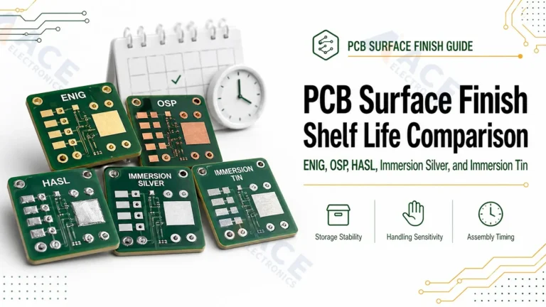
If you are trying to reduce PCB cost without changing the board design, OSP may look attractive.
It is low-cost, lead-free, and suitable for many volume PCB assembly projects. But it also gives you less room for long storage, repeated reflow, rough handling, or uncertain assembly schedules.
The short answer: OSP is a thin organic coating applied over exposed copper pads to prevent oxidation before soldering. It works well when the PCB will move quickly from fabrication to assembly. It becomes risky when boards may sit in storage for months, travel through humid environments, or need multiple reflow and rework cycles.
For a broader comparison of all common finishes, read our guide on how to choose PCB surface finish. This article focuses only on OSP.
Quick Answer: What Is OSP?
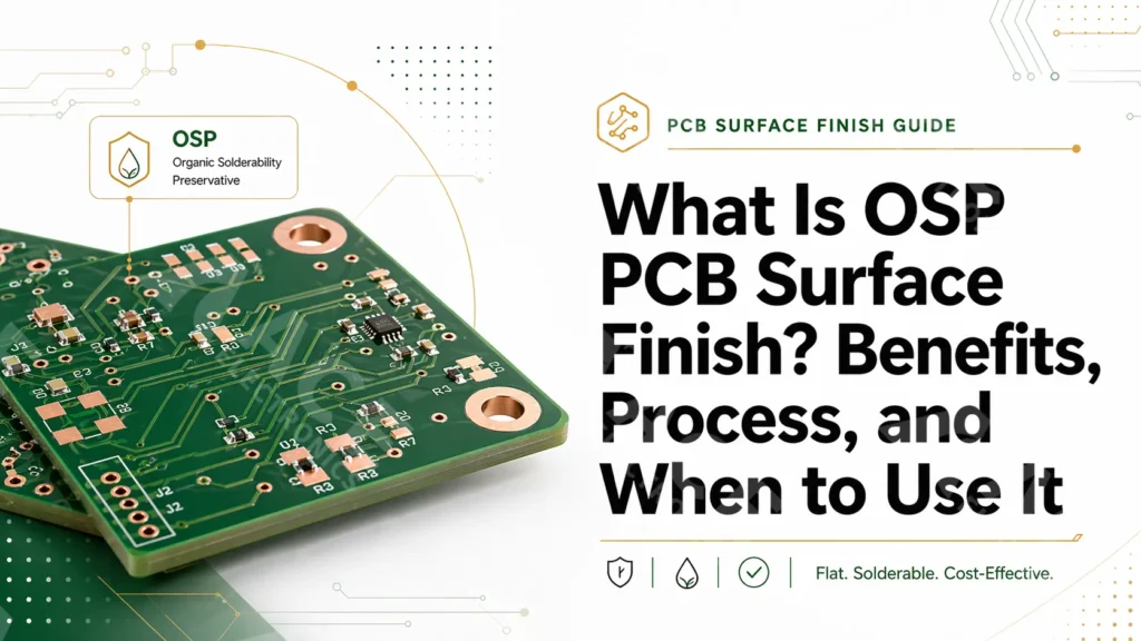
OSP stands for Organic Solderability Preservative.
It is a PCB surface finish that protects exposed copper pads with a very thin organic film. During soldering, this film is removed by heat and flux, allowing solder to bond directly to the copper.
| Item | Simple explanation |
|---|---|
| Full name | Organic Solderability Preservative |
| Surface type | Organic, non-metallic finish |
| Applied on | Exposed copper pads |
| Main purpose | Protect copper from oxidation before assembly |
| Main advantage | Low cost and very flat surface |
| Main limitation | Shorter practical storage and handling window |
| Best fit | Cost-sensitive boards assembled soon after fabrication |
| Use with caution | Long storage, uncertain assembly schedule, repeated reflow, heavy rework |
OSP is not a premium finish like ENIG. It is also not just a "cheap finish." It is a good choice when the project conditions match its strengths.
How OSP Works on a PCB
Bare copper solders well, but it oxidizes easily when exposed to air, moisture, fingerprints, or poor storage conditions. Once copper oxidizes, solderability becomes less predictable.
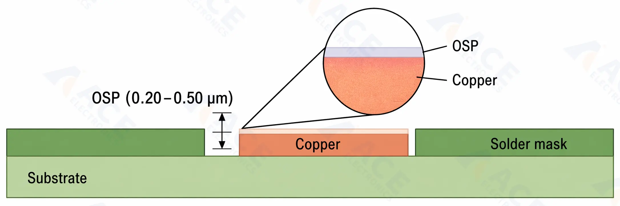
OSP protects exposed copper pads with a thin organic layer before soldering.
OSP solves this by forming a thin protective organic layer on the copper surface.
The basic process is:
- The PCB copper pads are cleaned.
- The copper surface is micro-etched and prepared.
- The board is dipped into an OSP chemical solution.
- The organic coating bonds to the exposed copper.
- The PCB is dried and packaged for storage or assembly.
Unlike HASL, OSP does not add a solder layer. Unlike ENIG, it does not add nickel or gold. It simply protects the copper until the board is ready for soldering.
During SMT reflow, the coating breaks down and the solder paste wets the copper pad directly.
Why Buyers Choose OSP
OSP is usually selected for practical manufacturing reasons, not because it looks impressive on a specification sheet.
1. Lower PCB Cost
Cost is the main reason many buyers consider OSP.
OSP has a simpler process than ENIG and does not use gold or nickel. For high-volume PCB orders, this cost difference can matter, especially in consumer electronics, simple industrial boards, and products with tight BOM targets.
If your PCB has no special reliability requirement and will be assembled quickly, OSP can be a reasonable way to reduce bare board cost.
2. Flat Surface for SMT Assembly
OSP creates a very flat surface because it does not build thick metallic layers on top of the copper pads.
This is useful for SMT components where pad flatness matters, including:
- Fine-pitch ICs
- QFN packages
- Small passive components
- Dense SMT layouts
- Some BGA designs, when the process is well controlled
Flatness is one reason OSP can work better than HASL for some SMT boards. However, for high-reliability BGA, fine-pitch, or uncertain storage conditions, ENIG PCB surface finish is often safer.
3. Lead-Free and Environment-Friendly
OSP is lead-free and compatible with lead-free assembly processes.
Because it is an organic coating rather than a metallic finish, it avoids some environmental concerns linked with older surface finish processes. This makes it attractive for products that need RoHS-compliant manufacturing.
4. Good Fit for Volume Production
OSP is often used when the production flow is stable:
- PCB fabrication schedule is clear
- SMT assembly happens soon after PCB delivery
- Storage time is short
- Handling is controlled
- Product design is already mature
- Rework rate is low
In this kind of production, OSP can support both cost control and stable soldering.
Where OSP Works Best
OSP is a good fit when the board is cost-sensitive and the assembly plan is predictable.
Use OSP when most of these conditions are true:
| Project condition | OSP fit |
|---|---|
| High-volume production | Good fit |
| Cost-sensitive product | Good fit |
| Short storage before assembly | Good fit |
| Stable SMT process | Good fit |
| Few rework cycles expected | Good fit |
| No edge connector wear requirement | Good fit |
| No wire bonding requirement | Good fit |
| Controlled packaging and handling | Good fit |
Typical applications may include:
- Consumer electronics
- Smart home products
- IoT control boards
- General industrial control boards
- LED controller boards
- Simple communication modules
- Mature products moving into repeat production
For these projects, OSP can be a practical finish if the PCB supplier and assembly supplier are aligned on timing, packaging, and soldering process control.
Main Limitations of OSP
OSP has real advantages, but buyers should understand the trade-offs before choosing it.
1. Shorter Practical Shelf Life
OSP is more sensitive to storage than ENIG or HASL.
The exact shelf life depends on the OSP chemistry, packaging, humidity, temperature, and handling conditions. In practical sourcing discussions, many buyers treat OSP as a finish that should be assembled relatively soon after fabrication.
If your boards may sit for months before assembly, OSP becomes less attractive.
This matters when:
- Components have long lead times
- PCB fabrication and assembly are handled by different suppliers
- Boards are shipped internationally before assembly
- The project schedule may change
- The customer wants to keep bare PCB inventory
If the schedule is uncertain, ENIG is usually safer.
2. More Sensitive to Handling
OSP is thin and transparent. It is not easy to inspect visually.
Fingerprints, moisture, scratches, poor packaging, or repeated handling can reduce solderability. This is especially important when boards move between multiple suppliers or are opened, inspected, repacked, and stored again.
For OSP boards, handling discipline matters.
3. Limited Tolerance for Multiple Reflow Cycles
OSP is consumed during soldering.
A simple single-sided SMT process is usually easier to manage. A double-sided assembly with multiple reflow cycles needs more attention. If the board also needs selective soldering, hand soldering, or repeated repair, OSP may become less stable than a metallic finish.
This does not mean OSP cannot support double-sided assembly. It means the process window is narrower.
4. Not Good for Long-Term Contact Surfaces
OSP is not suitable for wear surfaces.
Do not use OSP for:
- Gold fingers
- Edge connectors
- Keypad contacts
- Repeated insertion contacts
- Sliding contacts
- Wire bonding pads
For these features, a different finish such as hard gold or ENEPIG may be required.
OSP vs ENIG vs HASL: Quick Buyer View
This is only a quick buyer comparison. For a full surface finish selection overview, use our PCB surface finish guide.
| Finish | Best for | Main benefit | Main risk |
|---|---|---|---|
| OSP | Cost-sensitive boards assembled quickly | Low cost, flat, lead-free | Shorter storage and handling window |
| ENIG | BGA, fine-pitch, high-reliability PCBA | Flat, stable, better shelf life | Higher cost |
| HASL | Simple boards with larger pads | Low cost, familiar process | Less flat, not ideal for fine-pitch SMT |
A simple rule:
- Choose OSP when cost matters and assembly timing is controlled.
- Choose ENIG when reliability, BGA, fine-pitch, or storage risk matters.
- Choose HASL when the board is simple and pad flatness is not critical.
If your project has BGA or fine-pitch parts, also read our guide to best PCB surface finish for BGA assembly.
When You Should Avoid OSP
Avoid OSP if the board may face uncontrolled storage or complex assembly risk.
You should be cautious with OSP when:
- The PCB may be stored for a long time before assembly
- Component lead times are uncertain
- The product may require multiple reflow cycles
- Rework or hand soldering is expected
- The PCB will travel through humid shipping conditions
- The board uses important BGA or fine-pitch packages
- The product is used in medical, automotive, aerospace, or harsh industrial environments
- The cost of failure is much higher than the cost saved by OSP
- The design includes edge contacts or wear surfaces
For prototype and NPI builds, OSP can also be risky if the assembly process is not yet stable. Early builds often involve design changes, rework, schedule delays, and unexpected component substitutions. In those cases, ENIG may give the project more process tolerance.
Is OSP Good for BGA Assembly?
OSP can be used with BGA in some controlled production environments because it provides a flat copper surface.
But for many custom PCBA projects, especially prototypes, NPI builds, or lower-volume export projects, ENIG is often the safer starting point.
The reason is not only pad flatness. The real question is process control.
BGA assembly risk depends on:
- Pad design
- PCB flatness
- Solder paste printing
- Reflow profile
- Moisture control
- X-ray inspection
- Rework requirement
- Storage time before assembly
If the BGA is important to product reliability, do not choose OSP only because it is cheaper. Review the whole assembly plan first.
Questions to Ask Before Choosing OSP
Before approving OSP on a PCB quotation, ask these questions:
- How soon will the PCB be assembled after fabrication?
- Will the boards be stored before assembly?
- Will the boards be shipped internationally before SMT?
- Does the board have BGA, QFN, LGA, CSP, or fine-pitch ICs?
- Is the assembly single-sided or double-sided?
- How many reflow cycles are expected?
- Is hand soldering or rework likely?
- Will the product be used in a high-reliability market?
- How will the supplier package and store the OSP boards?
- Is the cost saving worth the narrower process window?
If you cannot answer these questions clearly, OSP may still work, but the decision is not ready yet.
What to Specify in Your PCB Fabrication Notes
If you choose OSP, do not leave the finish requirement vague.
Your fabrication notes may include:
- Surface finish: OSP
- Lead-free assembly requirement
- Applicable IPC or customer standard, if required
- Packaging requirement
- Storage requirement
- Maximum storage time before assembly, if controlled by your process
- Handling requirement
- Assembly schedule requirement
For high-temperature lead-free OSP, IPC-4555 is commonly referenced as the performance specification for high-temperature OSP on printed boards. The exact requirement should be confirmed with your PCB supplier and end-customer quality standard.
What ACE Usually Recommends
At ACE Electronics, we do not recommend surface finish only by unit price.
For cost-sensitive, stable, high-volume projects, OSP can be a good choice. It is especially reasonable when the PCB will be assembled soon after fabrication and the process has already been proven.
For BGA, fine-pitch, high-reliability, long-storage, or uncertain-schedule projects, we usually review ENIG first because it gives more process tolerance.
Before production, we can review your Gerber files, BOM, pick-and-place file, assembly notes, storage plan, and target delivery schedule. The goal is simple: choose the finish that supports both cost and assembly reliability.
If you need one supplier to manage PCB fabrication, component sourcing, SMT assembly, testing, and shipment, ACE can support your project as a turnkey PCBA factory. For real production examples, see our turnkey PCB assembly case study.
Final Recommendation
OSP is a good low-cost PCB surface finish when the production flow is controlled.
Use it when:
- Cost matters
- The board will be assembled quickly
- Storage time is short
- Handling is controlled
- The SMT process is stable
- The product does not need long-term contact durability
Avoid it when:
- The schedule is uncertain
- Boards may sit in inventory
- Multiple reflow or rework cycles are likely
- The product has high reliability requirements
- The cost of failure is higher than the cost saved
The best way to choose OSP is not to ask, "Is OSP good or bad?"
A better question is:
Can your PCB fabrication, storage, shipping, and assembly process stay inside the OSP process window?
If yes, OSP can reduce cost without creating unnecessary risk. If not, ENIG or another finish may be the better choice.
Frequently Asked Questions
What does OSP stand for in PCB?
What does OSP stand for in PCB?
OSP stands for Organic Solderability Preservative. It is a thin organic coating used to protect exposed copper pads before soldering.
Is OSP a good PCB surface finish?
Is OSP a good PCB surface finish?
Yes, OSP is a good PCB surface finish for cost-sensitive boards that will be assembled soon after fabrication. It is less suitable for long storage, heavy rework, or uncertain assembly schedules.
Is OSP cheaper than ENIG?
Is OSP cheaper than ENIG?
Yes. OSP is usually cheaper than ENIG because it does not use nickel or gold and has a simpler surface finish process.
Is OSP suitable for BGA?
Is OSP suitable for BGA?
OSP can be used for some BGA assemblies under controlled conditions, but ENIG is often safer for BGA, fine-pitch, prototype, NPI, and high-reliability projects.
How long can OSP PCBs be stored?
How long can OSP PCBs be stored?
OSP shelf life depends on chemistry, packaging, humidity, temperature, and handling. In practical production planning, OSP should be assembled relatively soon after PCB fabrication. If long storage is expected, ENIG is usually safer.
What is the main disadvantage of OSP?
What is the main disadvantage of OSP?
The main disadvantage is its narrower process window. OSP is more sensitive to storage, handling, moisture, multiple reflow cycles, and rework than many metallic finishes.
Is OSP lead-free?
Is OSP lead-free?
Yes. OSP is lead-free and commonly used for RoHS-compliant PCB assembly.
When should I avoid OSP?
When should I avoid OSP?
Avoid OSP when boards may be stored for a long time, handled by multiple suppliers, assembled after schedule delays, or used in high-reliability products where solderability risk is unacceptable.
About the Author
Bill Ho is Sales Engineer and Chief Editor at ACE Electronics, with 10 years of experience in PCB fabrication and PCB assembly.
He writes practical technical content focused on manufacturability review, fabrication communication, and assembly risk reduction.