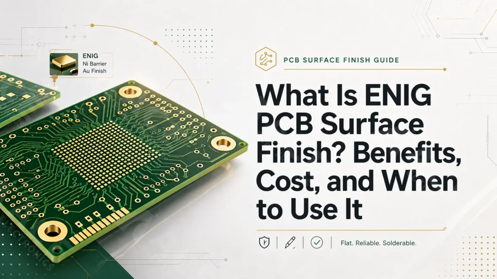
Many customers see ENIG in a PCB quotation and ask the same question: why is it more expensive?
The short answer: ENIG is a flat, reliable PCB surface finish often used for BGA, fine-pitch, and high-reliability PCB assemblies. It usually costs more than HASL or OSP, but in the right project, that extra cost can reduce soldering risk, storage risk, and long-term reliability problems.
Quick Answer: What Is ENIG?
ENIG stands for Electroless Nickel Immersion Gold.
It is a PCB surface finish made of two metallic layers:
| Layer | Role |
|---|---|
| Thin gold | Protects the nickel surface before soldering |
| Nickel | Works as the main solderable layer and barrier over copper |
ENIG is widely used because it gives PCB pads a flat, stable, and solderable surface. This makes it especially useful for BGA, QFN, fine-pitch SMT, and high-reliability PCBA projects.
When Should You Use ENIG?
| Project condition | Is ENIG recommended? | Why |
|---|---|---|
| BGA or QFN components | Yes | Flat pads help reduce assembly risk |
| Fine-pitch ICs | Yes | Better coplanarity than HASL |
| Industrial, medical, or automotive PCBA | Usually yes | Better long-term reliability |
| Long storage before assembly | Yes | Better shelf life than OSP |
| Simple through-hole PCB | Usually not necessary | HASL may be enough |
| Very cost-sensitive consumer product | Maybe not | OSP or HASL may reduce cost |
| High-volume, fast-turn assembly | Depends | OSP may work if timing is controlled |
For most BGA and fine-pitch projects, ENIG is a safe starting point.
How ENIG Works on a PCB
A bare PCB has exposed copper pads. Copper oxidizes easily, and oxidized copper is difficult to solder. The surface finish protects the copper until the board is assembled.
With ENIG, the PCB manufacturer first deposits a nickel layer over the copper pads. Then a very thin layer of immersion gold is applied over the nickel.
During soldering, the gold layer dissolves into the solder. The solder joint is mainly formed with the nickel layer underneath.
Typical ENIG thickness ranges are roughly:
| Layer | Common range |
|---|---|
| Gold | About 0.05-0.125 µm |
| Nickel | About 3-6 µm |
Exact thickness depends on the supplier, specification, and project requirements.
Why ENIG Costs More Than HASL or OSP
ENIG costs more because the process is more complex.
The cost usually comes from:
- Nickel and gold plating steps
- More process control
- More chemistry control
- More inspection requirements
- Higher material cost (Especially Gold)
- Tighter quality expectations for fine-pitch assembly
As a rough guide, ENIG may cost about 20-40% more than OSP for the surface finish portion. The final PCB price difference depends on board size, copper area, panel utilization, gold thickness, order quantity, and supplier pricing.
For a simple PCB, that extra cost may not be necessary. For a BGA or high-reliability PCBA, the better question is not only “Which finish is cheaper?” but “Which finish reduces assembly risk?”
Main Benefits of ENIG PCB Surface Finish
1. Flat Surface for BGA and Fine-Pitch Components
Flatness is one of the biggest reasons to choose ENIG.
BGA solder joints are hidden under the component body. If pad height is inconsistent, the risk of open joints, bridging, or poor solder collapse increases.
ENIG provides a much flatter surface than HASL, making it better for:
- BGA
- QFN
- LGA
- CSP
- Fine-pitch ICs
- HDI boards
- Dense SMT assemblies
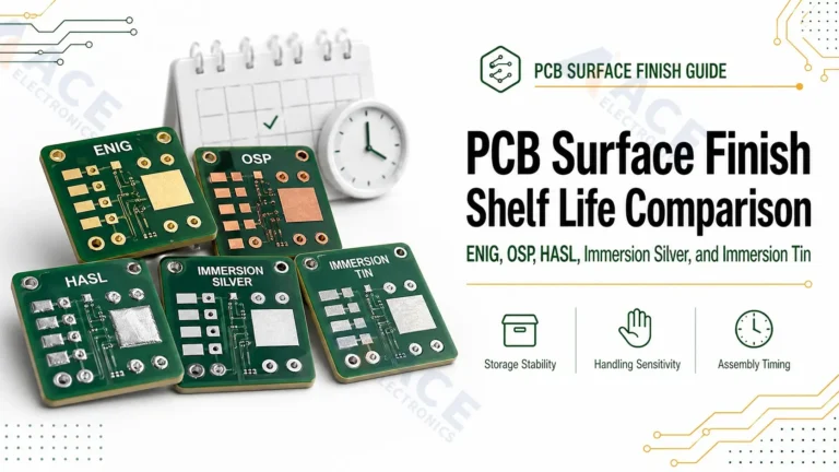
2. Better Shelf Life Than OSP
ENIG usually has a longer practical shelf life than OSP.
A common planning range is around 12 months under proper storage, and some suppliers may support longer shelf life depending on packaging and conditions.
This matters when:
- PCB fabrication and assembly are not done immediately
- Components have long lead times
- Boards need to be shipped internationally
- Production schedules may change
- The customer wants safer inventory control
OSP is more sensitive to storage and handling. If your supply chain timing is uncertain, ENIG is usually safer.
3. Good Solderability
ENIG gives a stable solderable surface when the plating process is well controlled.
This helps during:
- SMT assembly
- Lead-free reflow
- BGA placement
- Fine-pitch soldering
- Prototype and NPI production
Good solderability does not remove the need for correct PCB design, stencil design, solder paste control, and reflow profiling. But ENIG gives the assembly process a more stable starting point.
4. Suitable for High-Reliability Products
ENIG is commonly used in products where long-term reliability matters, such as:
- Industrial control boards
- Medical electronics
- Automotive electronics
- Communication modules
- Test and measurement equipment
- Payment terminals
- High-end consumer electronics
- Export PCBA projects
For these projects, the finish is not only a PCB cost item. It is part of the reliability strategy.
When ENIG May Not Be Necessary
ENIG is useful, but it is not always required.
You may not need ENIG if the board is:
- Simple through-hole assembly
- Large-pitch SMT only
- Low-density design
- Short-life consumer product
- Very cost-sensitive
- Assembled soon after PCB fabrication
- Free of BGA, QFN, or fine-pitch parts
In these cases, HASL or OSP may be enough.
For example, a simple relay control board with large pads and no fine-pitch ICs may not need ENIG. Paying extra for ENIG may not improve the final product enough to justify the cost.
Common ENIG Risks to Know
ENIG is not perfect. Buyers should understand the risks before choosing it.
Higher Cost
ENIG is usually one of the more expensive common PCB surface finishes. If the board is simple and cost is the main concern, it may be over-specified.
Black Pad Risk
Black pad is a known ENIG-related defect caused by poor plating process control. It can lead to weak solder joints and reliability problems.
This does not mean ENIG should be avoided. It means the PCB supplier must control the plating process properly.
For BGA and high-reliability projects, supplier quality matters.
Not Ideal for Every Mechanical Contact
ENIG is not the same as hard gold. If the design has edge fingers or contacts that require repeated insertion, hard gold may be needed instead.
ENIG vs Other PCB Surface Finishes
This article focuses on ENIG itself. For detailed comparisons, use dedicated comparison pages.
| Comparison | Simple takeaway |
|---|---|
| ENIG vs HASL | ENIG is flatter and better for BGA; HASL is cheaper and good for simpler boards |
| ENIG vs OSP | ENIG has better shelf life and handling tolerance; OSP is cheaper and very flat |
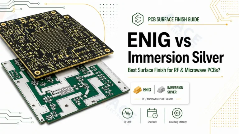
| ENIG vs Immersion Silver | Both are flat; immersion silver is more sensitive to tarnishing and storage |
| ENIG vs Hard Gold | ENIG is for solderable pads; hard gold is for wear-resistant contacts |
How to Decide If Your PCB Needs ENIG
Use this checklist before confirming the surface finish.
Choose ENIG if you answer “yes” to any of these questions:
- Does the PCB have BGA, QFN, LGA, CSP, or fine-pitch ICs?
- Is the smallest pitch 0.5 mm or below?
- Is the product used in industrial, medical, automotive, or outdoor environments?
- Will the PCB be stored before assembly?
- Are component lead times uncertain?
- Does the assembly require multiple reflow or rework steps?
- Is the cost of failure much higher than the cost of the surface finish?
- Is this a new design going through prototype or NPI?
- Does the customer require stronger quality confidence?
If the answer is yes, ENIG is usually worth considering.
What We Usually Recommend at ACE Electronics
For most BGA, QFN, fine-pitch, and high-reliability PCBA projects, ACE Electronics usually recommends ENIG as the default starting point.
It is especially suitable for:
- Prototype and NPI builds
- High-density SMT assembly
- Industrial control PCBA
- Medical electronics
- Automotive electronics
- Communication modules
- Export projects for Europe and North America
If your project is simple and cost-sensitive, we may recommend another surface finish instead. The right choice depends on the component package, storage time, assembly process, reliability requirements, and budget.
Before production, we can review your Gerber files, BOM, pick-and-place file, and assembly notes to check whether ENIG is necessary.
Related Guides and Services
For getting quote of PCB fabrication, check PCB Fabrication Service
For a broader overview of PCB surface finishes, read: How to Choose PCB Surface Finish
For BGA and fine-pitch assembly, see: SMT Assembly Service
For full project support, see: Turnkey Assembly Services
Frequently Asked Questions
What does ENIG stand for?
What does ENIG stand for?
ENIG stands for Electroless Nickel Immersion Gold.
Is ENIG good for BGA?
Is ENIG good for BGA?
Yes. ENIG is one of the most common choices for BGA assembly because it provides a flat and stable solderable surface.
Why is ENIG more expensive?
Why is ENIG more expensive?
ENIG uses nickel and gold plating steps, requires tighter process control, and usually has higher inspection requirements than simpler finishes such as HASL or OSP.
How long is ENIG shelf life?
How long is ENIG shelf life?
A common planning range is around 12 months under proper storage. Actual shelf life depends on supplier specification, packaging, humidity, temperature, and handling.
Is ENIG better than HASL?
Is ENIG better than HASL?
For BGA, QFN, fine-pitch, and high-density SMT boards, ENIG is usually better because it is flatter. For simple boards, HASL may be enough and cheaper.
Is ENIG better than OSP?
Is ENIG better than OSP?
ENIG is usually better for storage, handling, and high-reliability projects. OSP can be better for low-cost, high-volume, fast-turn production if the assembly window is controlled.
Do all PCBs need ENIG?
Do all PCBs need ENIG?
No. Simple PCBs without fine-pitch parts may not need ENIG. The choice should depend on assembly risk, reliability requirements, storage time, and cost target.
About the Author
Bill Ho is Sales Engineer and Chief Editor at ACE Electronics, with 10 years of experience in PCB fabrication and PCB assembly.
He writes practical technical content focused on manufacturability review, fabrication communication, and assembly risk reduction.