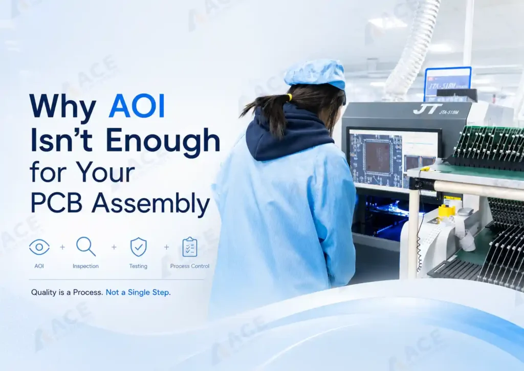
Automated optical inspection (AOI) is a quality step used at two stages in PCB production. During PCB fabrication, AOI checks bare boards for trace width violations, shorts, opens, and excess copper. During PCB assembly, after SMT reflow, the system uses cameras and image processing software to check each assembled board for visible defects — missing components, solder bridges, tombstoning, wrong polarity, or lifted leads. For many production runs, this optical check is the primary gate before a board moves further downstream.
But 2D AOI alone cannot guarantee a good PCBA. It only sees the surface from above. It cannot see under a BGA, inside a connector body, or behind a large component.
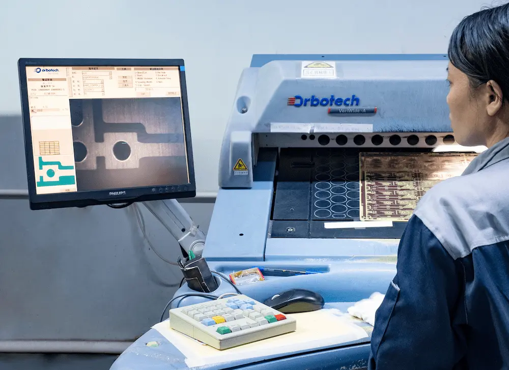
A technician inspects a bare PCB on an AOI machine during PCB fabrication. At this stage, the system checks for trace width violations, shorts, opens, and excess copper before the board moves to assembly.
3D AOI adds height measurement — it can check solder volume on QFN thermal pads and connector fillets — but it still cannot see through a component body. Only X-ray can inspect the hidden joints beneath BGA, CSP, and LGA packages.
This article explains what automated optical inspection for PCB assembly actually verifies, what it misses, and what buyers and engineers should check before approving a production run.
What Is AOI in PCB Assembly?
AOI stands for automated optical inspection. In PCB assembly, it is a machine-vision system that captures high-resolution images of an assembled board and compares each placement, solder joint, and visible feature against a reference — either CAD data or a known-good golden board.
The system flags differences that exceed programmed thresholds. Most automated checks happen after reflow soldering in SMT assembly, though some lines also position optical inspection after solder paste printing and before reflow.
Where AOI Fits in a PCBA Production Line
A typical SMT production sequence places AOI at two possible points — before and after reflow:
- Solder paste printing — paste is deposited onto PCB pads through a stencil
- SPI (solder paste inspection) — a separate inline system checks paste volume, height, and offset before placement
- Pick-and-place — components are placed onto the paste deposits
- AOI before reflow — the machine images the board before it enters the reflow oven to catch missing parts, wrong polarity, component shift, or reversed orientation while they are still easy to remove
- Reflow soldering — the board passes through a controlled thermal profile to form solder joints
- AOI after reflow — the assembled board is imaged again to check solder joint quality: bridging, tombstoning, insufficient solder, and lifted leads
- Post-AOI steps — depending on the product, these may include X-ray, ICT, functional testing, conformal coating, or final product assembly
Each step catches problems from the previous one. SPI catches paste printing issues before components are placed. Optical inspection catches visible soldering and placement issues before the board moves further downstream. X-ray and functional testing catch what the cameras cannot.
For a closer look at how each step is set up and controlled in production, see ACE Electronics's SMT assembly services.
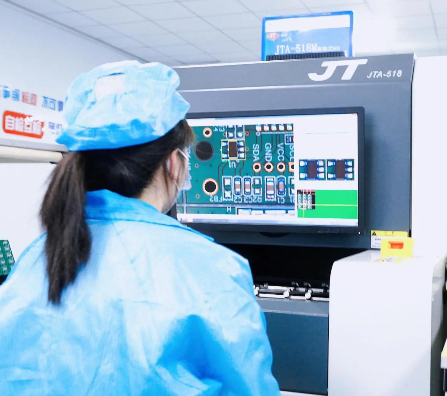
An AOI station inspects assembled PCBAs after SMT reflow. The system compares every component position and solder joint against CAD data or a golden board reference to flag visible defects before the boards move to X-ray or functional testing.
How AOI Inspects a PCB Assembly
The inspection system uses multiple cameras, controlled lighting angles, and image analysis algorithms to evaluate every placement position on the board.
Cameras, Lighting, and Image Comparison
The system illuminates the board from different angles — typically top-down, angled, and side lighting — to create multiple image layers. Each capture is compared pixel by pixel against the reference. Differences in shape, color, brightness, or position trigger a flag.
How Modern AOI Systems Build the Inspection Program
Most AOI machines installed after 2015 no longer require a physical golden board.
| Reference Method | How It Works in Practice | How Common It Is |
|---|---|---|
| CAD / ODB++ Import | The software reads Gerber, CAD placement coordinates, and BOM directly. Component shapes, pad positions, and polarity marks are mapped automatically. The engineer only reviews exceptions where the library lacks a matching footprint. | Standard for 90%+ of new products |
| AI / Deep Learning | The machine inspects 20–50 known-good boards to learn normal variation in solder shape, component placement, and pad wetting. It then flags outliers without a rigid CAD reference. | Growing; standard on newer Koh Young, Mirtec, and some Chinese AOI lines |
| Algorithmic Rules | The programmer sets geometric thresholds (e.g., solder fillet must cover 75% of pad, component must sit within ±0.05 mm of center). The machine judges each joint against IPC-A-610 criteria rather than a reference image. | Common for simple passives and standard packages |
| Golden Board | A known-good assembled board is scanned and saved as the master image. Every subsequent board is compared pixel-by-pixel. | Rare today; used only for legacy products without CAD data or stable repeat orders where the design never changes |
2D AOI vs 3D AOI
| Feature | 2D AOI | 3D AOI |
|---|---|---|
| What it measures | Top-down pattern, color, shape | Height, volume, coplanarity, solder fillet profile |
| Light source | Single or multi-angle LED | Structured light, laser, or multi-angle stereo |
| Good for | Missing components, polarity, bridging, basic offset | Solder joint quality, coplanarity, lifted leads, insufficient solder volume |
| Limitation | Cannot assess solder joint height or volume | Higher cost, slower cycle time on some systems |
Many production lines use 2D AOI for standard consumer PCBA orders, and add 3D AOI when the products require stricter solder joint verification, such as automotive and industrial devices.
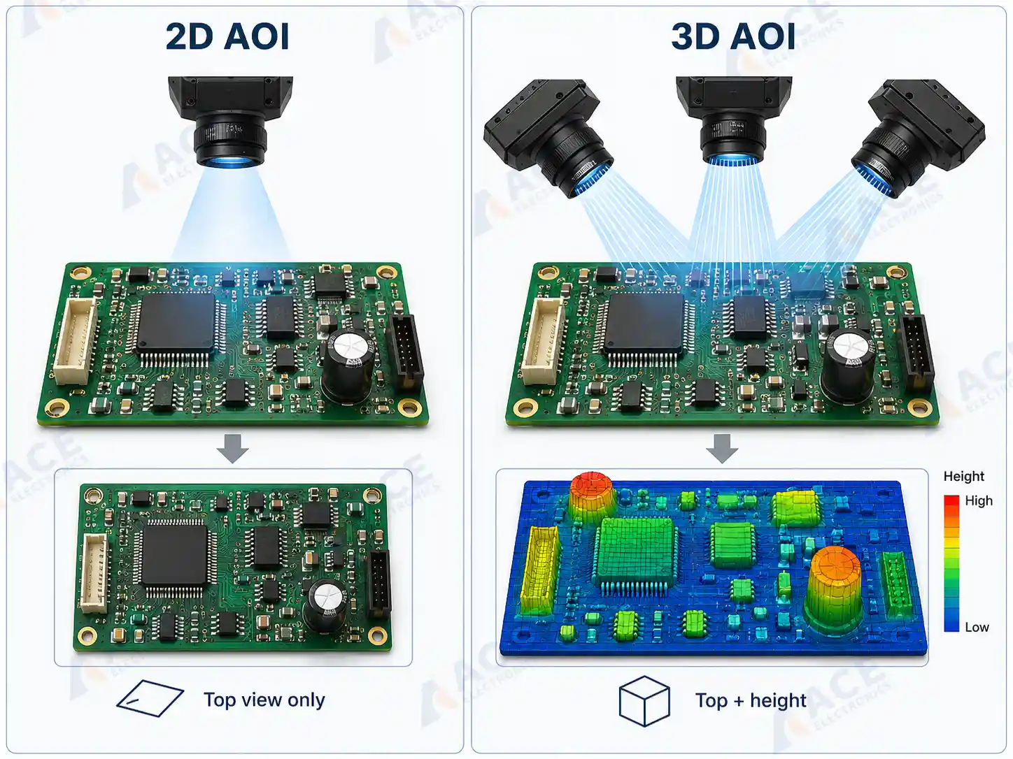
2D AOI captures a flat top-down image and compares it against a reference pattern. 3D AOI adds height measurement using structured light, allowing the system to check solder volume, fillet shape, and component coplanarity — not just whether the part is present.
What AOI Can Detect on a PCBA
The system reliably catches visible assembly defects. Before a production run, the engineering team loads component locations, package types, polarity orientation, and acceptable tolerance ranges into the inspection program.
Defects AOI Catches Reliably
| Defect Type | What the Optical Check Sees | Why It Matters |
|---|---|---|
| Missing component | Empty pad where a component should be | Functional failure |
| Wrong component | Package shape, marking, or size mismatch | Incorrect circuit behavior |
| Polarity reversal | Component orientation reversed (diode, LED, capacitor, IC) | Immediate or delayed failure |
| Solder bridging | Solder connecting adjacent pads or pins | Electrical short |
| Tombstoning | One end of a chip component lifted off the pad | Open circuit |
| Component offset | Part shifted beyond acceptable X/Y tolerance | Partial connection or short |
| Insufficient solder | Incomplete fillet or thin joint | Weak connection, intermittent failure |
| Lifted lead | A lead not coplanar with the pad | Open circuit |
| Wrong orientation | Component rotated from intended placement | Functional failure |
| Solder balls | Small solder spheres near pads | Short risk, contamination |
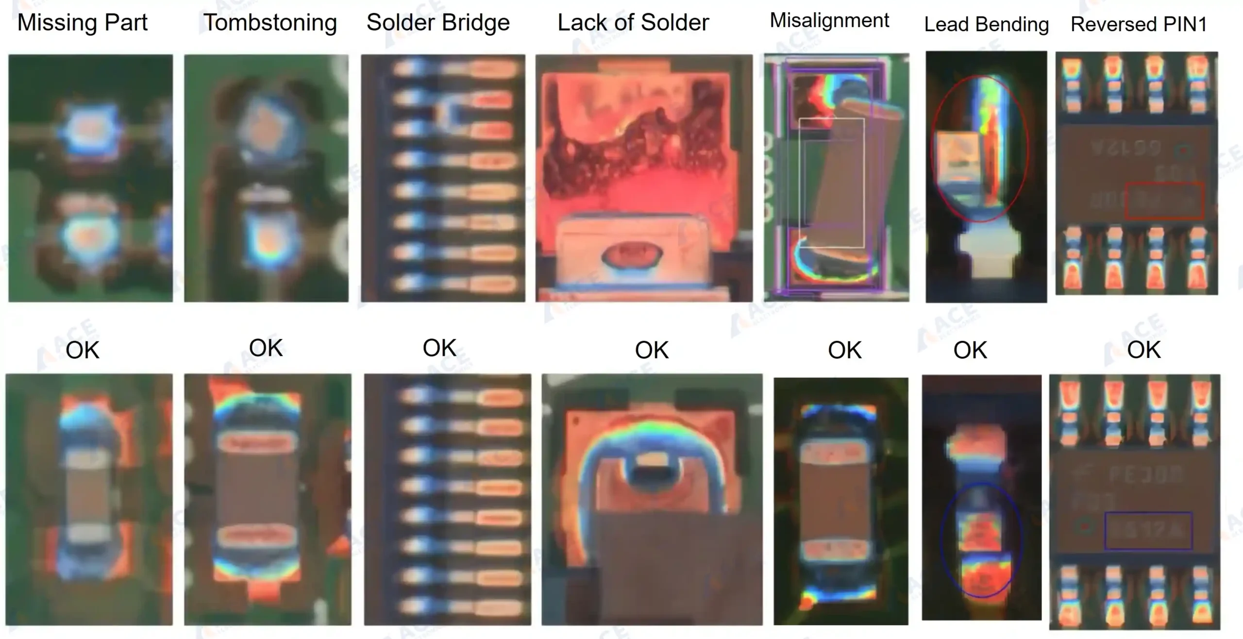
Actual assembly defects flagged by a 2D AOI system on a production PCBA. These include missing components, wrong component orientation, solder bridging between adjacent pads, tombstoning, and component shift — all visible from a top-down camera angle.
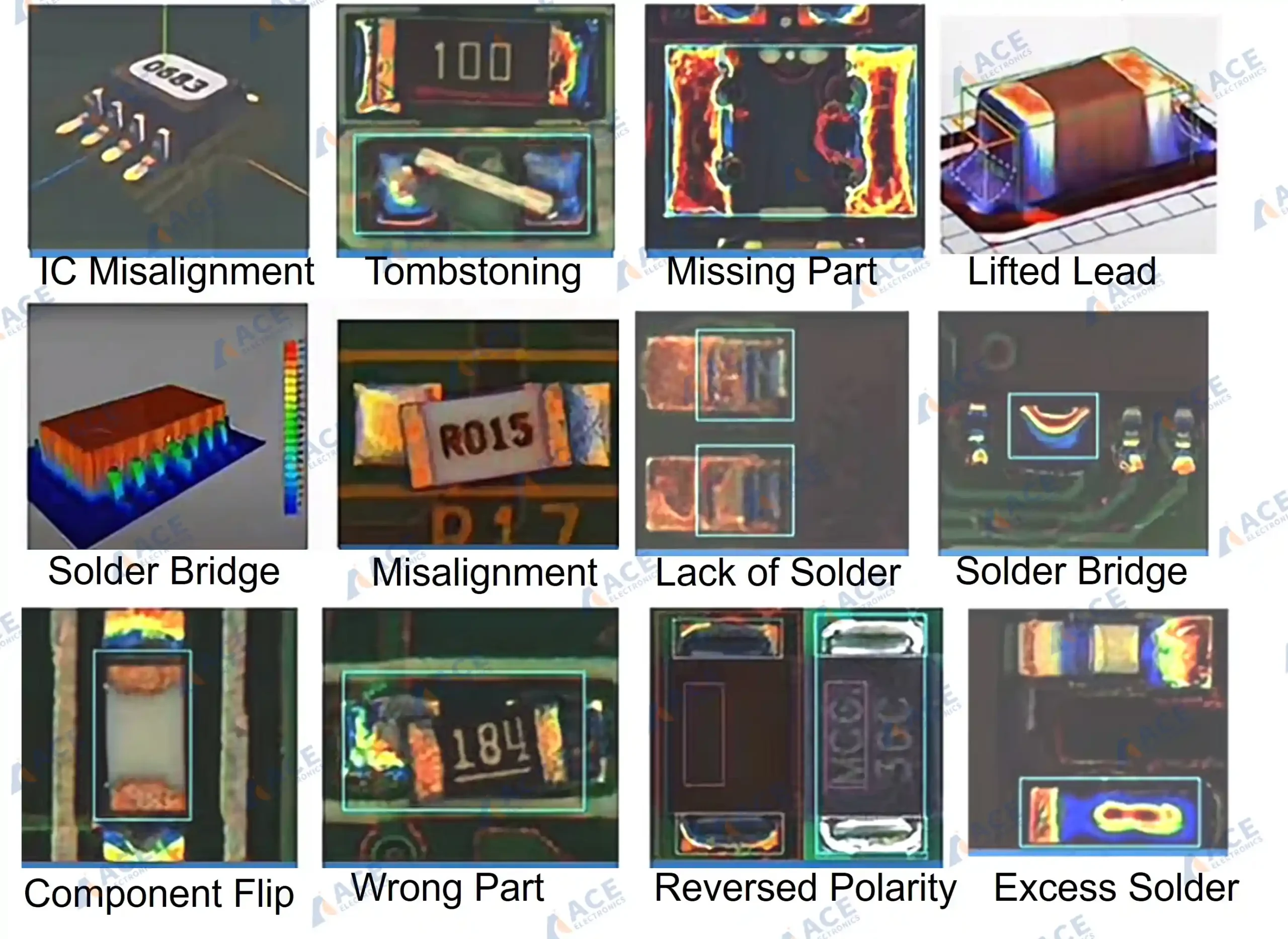
Defects that 3D AOI can catch that 2D AOI may miss: insufficient solder volume on a QFN thermal pad, a lifted lead where one side sits higher than the pad, and a solder fillet with abnormal height — all detectable through height and volume measurement.
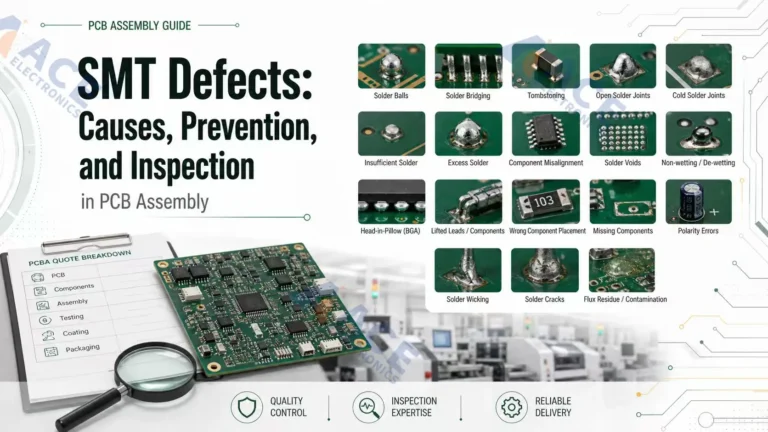
For a deeper review of each defect type — causes, prevention, and process control — see the SMT defects guide.
What AOI Cannot See — and Why That Matters
Hidden Solder Joints Under BGA and LGA Packages
A BGA or LGA package hides every solder joint under the component body. Optical inspection can confirm the part is centered and oriented correctly, but it cannot see through the package to judge wetting, voiding, bridging, or head-in-pillow defects on the solder balls beneath.
Only X-ray can see through the component body to evaluate these hidden joints.
Internal Voids and Head-in-Pillow Defects
Solder voids are gas cavities trapped inside a solder joint. Head-in-pillow is a hidden defect where the BGA ball and solder paste make contact but do not fully merge into one reliable joint. Both pass optical inspection because the package body and visible edges look normal from above.
Optical inspection and X-ray are complementary. The camera-based check handles visible surfaces quickly and at production speed. X-ray covers the hidden joints beneath components. Neither replaces the other.
When Is 100% AOI Required? Prototype Runs vs Volume Production
How much optical inspection you need depends on order size, component pitch and density, and the cost of a field failure. Below is how coverage decisions change between first-time builds and repeat high-volume orders.
Prototypes and First Article Inspection (FAI)
On prototype and new product introduction (NPI) runs, every board is inspected — 100% coverage, every placement. Combined with first article inspection (FAI), this gives fast feedback on whether the assembly setup matches the design files.
The first few boards often reveal placement rotation errors, missing parts, or polarity mistakes that the pick-and-place program, BOM, or assembly drawing did not catch. Fixing these on board 3 is far cheaper than discovering them after the full batch is built.
High-Volume Production: 100% or Sampled AOI?
In repeat production with a validated process, some suppliers shift from 100% AOI to sampled inspection — checking a defined percentage of boards per lot. Whether this is acceptable depends on the product's risk level and the acceptance class.
Before you approve a volume quote, confirm whether inspection coverage is 100% or sampled. For automotive, medical, or any IPC-A-610 Class 3 product, 100% coverage should remain the default even at volume.
Our standard at ACE Electronics:
Whether it is a 5-board prototype or a 5,000-board production run, every single PCB assembly passes through AOI. We do not switch to sampled inspection at volume.
How AOI Connects to Other Inspections
It does not operate in isolation. On a well-controlled SMT line, multiple inspection gates feed into each other.
| Inspection Gate | What It Checks | How It Connects to AOI |
|---|---|---|
| SPI | Solder paste volume, height, area, offset | Paste defects flagged here help explain AOI findings after reflow |
| AOI | Visible placement and soldering defects | Catches what SPI cannot predict |
| X-ray | Hidden BGA/QFN joints, voids, head-in-pillow | Covers the joints AOI cannot see |
| ICT | Opens, shorts, component values | Electrical confirmation of assembly quality |
| FCT | Board functional operation | Verifies the PCBA works under power and signal conditions |
IPC-A-610 Acceptance Classes and Optical Inspection
Optical inspection pass/fail rules are not universal. They are programmed based on the acceptance class that applies to the product:
| Acceptance Class | Typical Products | Inspection Tolerance |
|---|---|---|
| Class 1 | General consumer products | Wider tolerances; cosmetic defects may be accepted |
| Class 2 | Industrial, commercial, telecom | Stricter soldering and placement criteria |
| Class 3 | Automotive, medical, aerospace, high-reliability | Tightest tolerances; near-zero defect expectation |
What Buyers and Engineers Should Confirm About AOI
Before committing to a production order, here is a checklist of AOI-related questions worth confirming with the assembly partner:
| Question | Why It Matters |
|---|---|
| Is AOI included in the quoted assembly price, or is it optional? | Some suppliers quote assembly without inspection to look cheaper |
| Is AOI run at 100% coverage for every board, or is it sampled? | Prototype and high-reliability orders should default to 100% |
| Are both sides of the board inspected if the assembly is double-sided? | Some suppliers only inspect the primary side |
| What acceptance class are the inspection rules based on? | Confirms whether tolerances match the product's reliability needs |
| Is X-ray used for BGA, QFN, or other hidden joints? | Not all suppliers include X-ray; clarify whether it is available and when it is applied |
| Are AOI records or reports available if needed? | Useful for quality audits, failure analysis, and customer documentation |
For turnkey production orders where the assembly partner also manages component sourcing, PCB fabrication, and testing, confirming inspection coverage upfront prevents misunderstandings about what "inspected" means. See PCBA contract manufacturing for the scope typically covered in a turnkey workflow. For the procurement-side view — full vs partial turnkey and what to include in your RFQ — read the full turnkey PCB assembly guide.
Skipping AOI to Meet a Deadline — One Customer Almost Face the risk
We once quoted a 20-board prototype for a German automotive customer on 10th May 2026. He needed them delivered in two weeks. During the call, he mentioned another factory had promised one-week delivery — nearly half our timeline.
After double-checking the design files, we estimated that component sourcing and bare PCB fabrication alone would take at least 7 days. Incoming component inspection, SMT assembly, AOI programming, and full inspection would add another 2 to 4 days. That put us at 9 to 14 days — right at his deadline, but nowhere near one week.
There were some QFN components need to be soldered on his PCBs. The QFN solder joints sit under the package — cannot see them from any angle, not with a microscope and not with a camera. To deliver in one week, a factory would have to skip 3 important steps: machine pick-and-place and '3D AOI' and X-ray. That means they would plan to place parts by hand and shipping boards with no AOI or full inspection.
We told him honestly: one week is possible only if you agree to skip the inspection steps. We also suggested he ask the factory whether their one-week quote included machine 'pick and place', 3D AOI and X-ray inspection.
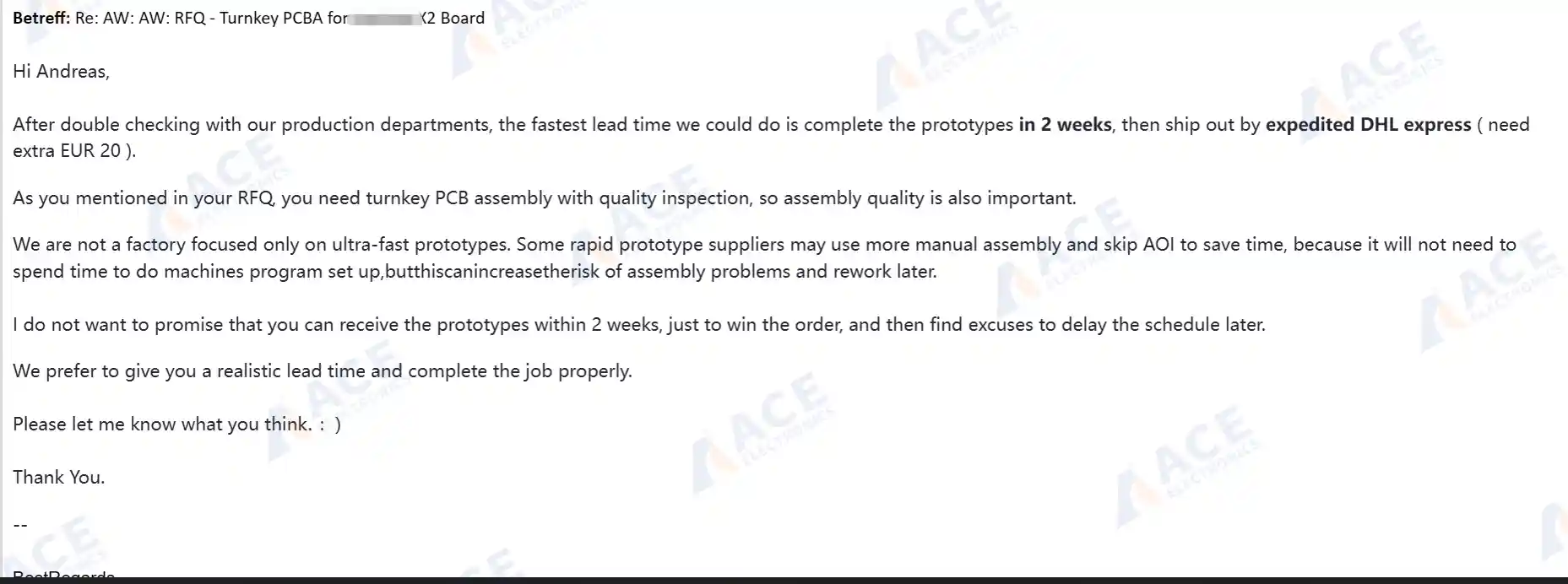
The email we sent to the customer. We broke down the real timeline — component sourcing, PCB fabrication, SMT assembly, and inspection — and explained why a one-week delivery would mean skipping AOI and X-ray for the QFN components on his board.
In the end, the customer agreed to our two-week timeline with full inspection — and placed the order with us.
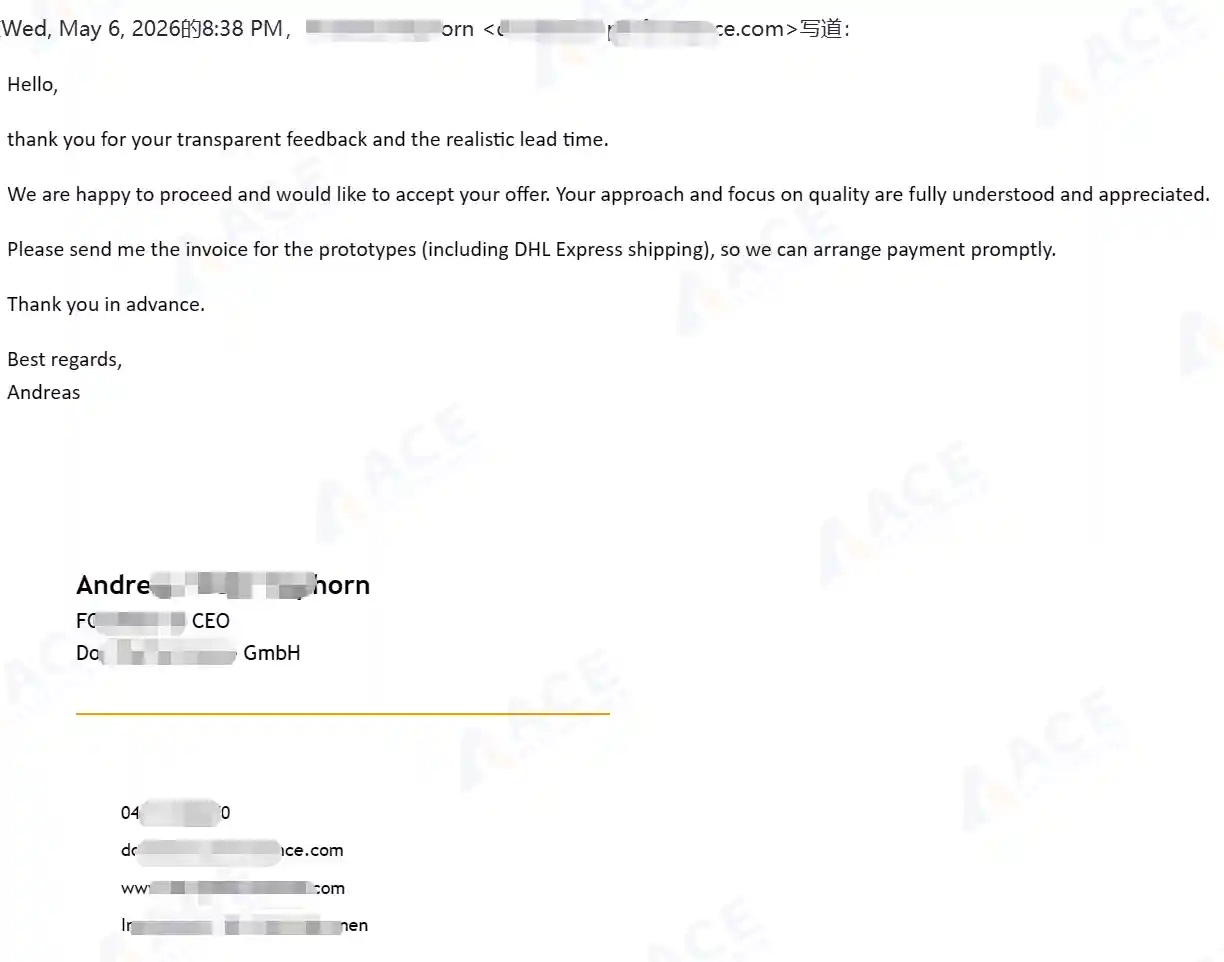
The customer's reply. After understanding what the shorter lead time would cost — no AOI, no X-ray, hand-placed QFN parts — he chose the two-week timeline with full inspection coverage.
A shorter lead time is not a better deal if it comes at the cost of skipping AOI. Before you accept a fast quote, confirm automated optical inspection is included — especially if your project serves industrial or automotive applications.
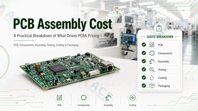
Inspection is one factor; many others shape the final quote. See what else drives PCB assembly cost before you compare proposals.
Conclusion
AOI is a reliable method for catching visible assembly defects on a PCBA. It verifies component presence, polarity, placement accuracy, and solder joint quality on exposed surfaces. But it stops where the camera stops.
A board that passes AOI still carries risk if it has BGA, QFN, LGA, or any package with hidden solder joints. Those risks can only be addressed by 3D AOI and X-ray inspection and confirmed by functional testing. AOI is not the end of the quality conversation — it is one gate in a longer inspection chain.
If your next PCB assembly order involves fine-pitch ICs, BGA packages, dense layouts, or high-reliability requirements, confirm inspection coverage with the assembly partner before production starts. If you need a production partner that reviews optical inspection, X-ray, FAI, and functional test requirements together — send your files and requirements for a review.
Frequently Asked Questions
What is AOI in PCB assembly?
What is AOI in PCB assembly?
AOI stands for automated optical inspection. In PCB assembly, it uses cameras and image processing software to check the assembled board for visible defects such as missing components, wrong polarity, solder bridges, tombstoning, and component misalignment after SMT reflow.
What is AOI in SMT assembly?
What is AOI in SMT assembly?
In SMT assembly, AOI is placed after reflow soldering. It captures images of the assembled PCB and compares each placement and solder joint against a reference — either CAD data or a known-good golden board — to flag visible assembly defects before the board moves to the next process step.
What defects can AOI detect on a PCBA?
What defects can AOI detect on a PCBA?
AOI reliably detects missing components, wrong component values or orientation, polarity errors, solder bridges, tombstoning, insufficient or excess solder, lifted leads, and visible placement offsets. It can also flag paste-related issues when combined with SPI feedback.
What is the standard for AOI inspection?
What is the standard for AOI inspection?
There is no single universal AOI standard. Instead, AOI pass/fail rules are set by the acceptance criteria defined for the product — typically IPC-A-610 Class 2 or Class 3 — combined with customer-specific requirements, golden board samples, and CAD data programmed into the AOI system.
Why is X-Ray inspection still needed if AOI is used?
Why is X-Ray inspection still needed if AOI is used?
AOI can only inspect visible surfaces. X-ray is needed for hidden solder joints — those under BGA balls, QFN thermal pads, and CSP packages. AOI cannot see internal solder voids, head-in-pillow defects, or bridging under a BGA. X-ray and AOI are complementary, not interchangeable.