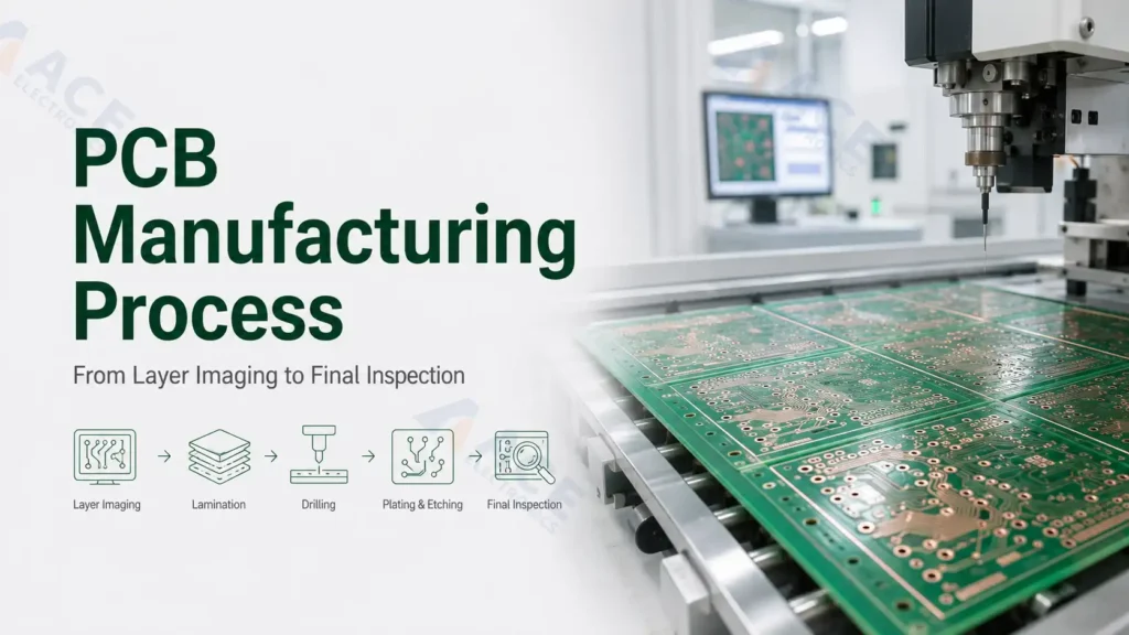
The PCB manufacturing process turns PCB layout design files into bare printed circuit boards that are ready for assembly. A typical printed circuit board manufacturing process includes file review, panelization, imaging, etching, lamination, drilling, copper plating, solder mask, surface finish, silkscreen, electrical testing, final inspection, and packing.
PCB manufacturing turns design data into a physical circuit board through a sequence of tightly controlled imaging, etching, lamination, drilling, plating, solder mask, and surface finish steps. These steps become more critical when the board has multiple layers, controlled impedance, fine-pitch components, plated through holes, tight mechanical tolerances, or specific surface finish requirements.
This guide focuses on how circuit boards are made at the bare PCB stage. It also explains where PCB fabrication details can affect later SMT assembly, through-hole assembly, testing, coating, and final product assembly.
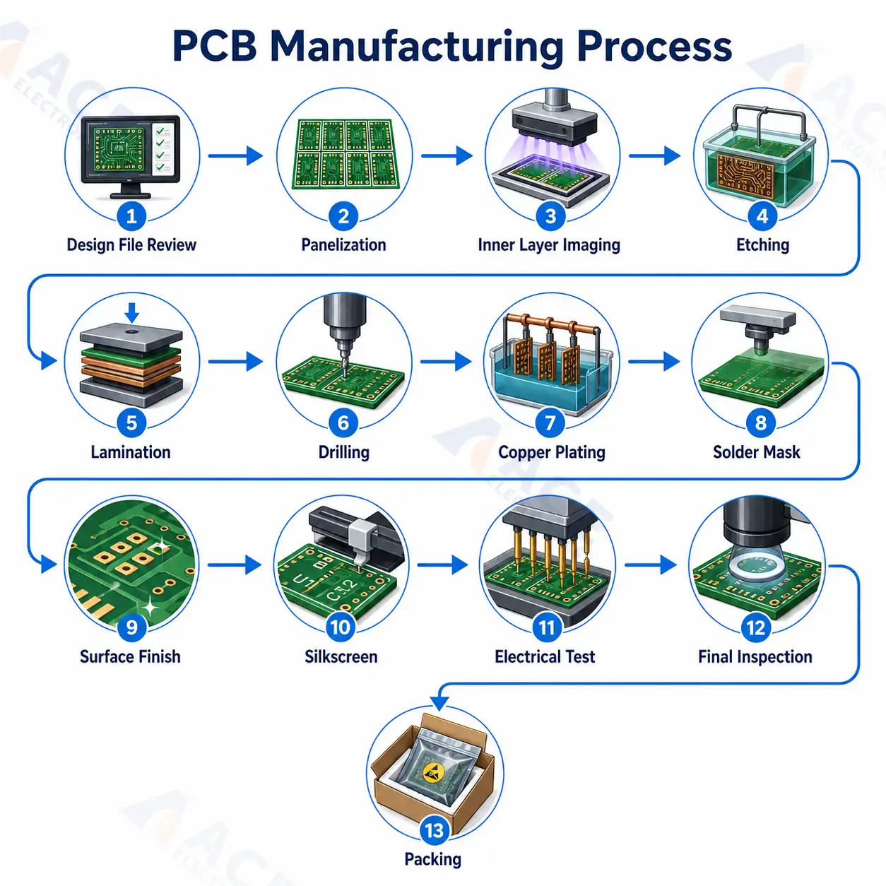 PCB manufacturing process flow chart showing DFM review, imaging, etching, lamination, drilling, plating, solder mask, surface finish, silkscreen, electrical testing, final inspection, and packing.
What Is the PCB Manufacturing Process?
The PCB manufacturing process is the controlled production flow used to convert PCB design data into a physical printed circuit board. The finished bare PCB provides copper circuits, insulating laminate, drilled holes, plated vias, pads, solder mask, silkscreen markings, and a solderable surface finish.
PCB manufacturing is same as PCB fabrication. In this guide, both refer to making the bare circuit board before components are mounted.
PCB assembly is the next stage, where components are placed and soldered onto the bare PCB to create a PCBA (assembled PCB).
What to Prepare Before PCB Manufacturing
Before a PCB factory can start production, the buyer should provide complete design and manufacturing data. Missing or unclear information is one of the most common reasons for quote delays, CAM questions, engineering holds, and avoidable revisions.
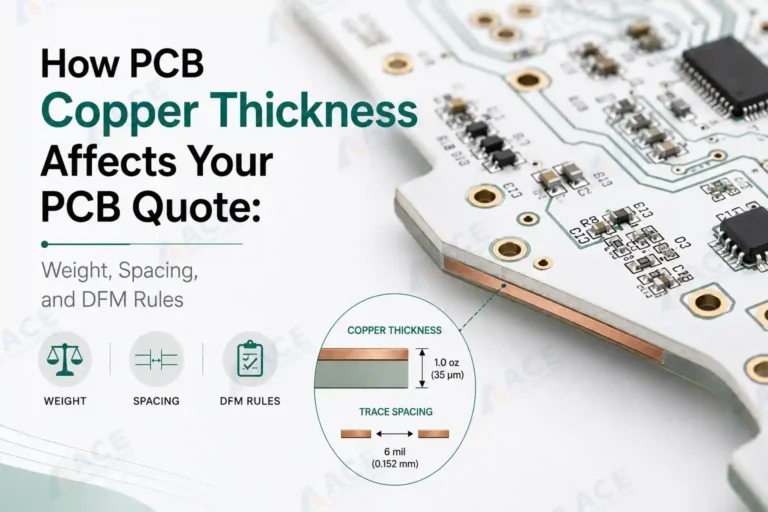
At minimum, a PCB manufacturing order usually needs Gerber or ODB++ data, NC drill files, a fabrication drawing, stack-up requirements, material requirements, board thickness, copper weight, surface finish, solder mask color, and any impedance or test requirements.
If the same order will continue to PCB assembly, the buyer should also prepare the BOM, pick-and-place file, assembly drawing, polarity notes, approved substitutions, and test instructions. For a practical file checklist, see our guide to Gerber, BOM, pick-and-place, and other PCB assembly files.
| File or specification | What it tells the PCB factory | Common issue if missing or unclear |
|---|---|---|
| Gerber files or ODB++ data | Shows the copper layers, solder mask, silkscreen, paste layers, and board outline | Wrong layer order, missing solder mask openings, unclear board profile |
| NC drill files | Shows plated holes, non-plated holes, vias, slots, and tooling holes | Wrong hole size, missing slots, unclear PTH/NPTH status |
| Stack-up requirement | Specifies layer order, dielectric thickness, copper weight, and impedance structure | Impedance variation, lamination risk, cost changes |
| Material requirement | Specifies FR-4, high-Tg FR-4, high-frequency laminate, flex material, aluminum substrate, or other base material | Wrong laminate selection, lead-time mismatch, reliability concerns |
| Surface finish requirement | Specifies HASL, lead-free HASL, ENIG, OSP, immersion silver, or another finish | Solderability risk, shelf-life issues, fine-pitch assembly limits |
| Test requirements | Specifies electrical testing, impedance coupons, inspection level, or additional reports | Hidden defects, missing records, unclear acceptance criteria |
| Assembly files | Supports PCBA quotation and production planning with BOM, placement, polarity, and testing information | BOM mismatch, placement errors, unclear polarity or test scope |
Early DFM and PCB layout support can help to catch manufacturability issues before releasing files for fabrication.
PCB Manufacturing Process Flow Chart
A PCB manufacturing process flow chart usually starts with DFM and engineering review and ends with tested bare boards packed for shipment or assembly. The exact process varies by board type, layer count, material, via structure, and inspection requirements, but a multilayer rigid PCB commonly follows this sequence.
| Stage | What happens | Common quality risk or order impact |
|---|---|---|
| DFM review and engineering checks | The factory checks Gerber files, drill files, stack-up, impedance, material requirements, and fabrication notes | Quote delays, engineering questions, wrong assumptions before production |
| CAM preparation and panelization | The design data is converted into production data, and boards are arranged into manufacturing panels | Poor material use, SMT handling issues, fixture mismatch, or depaneling problems |
| Inner layer imaging and developing | The circuit pattern for each inner copper layer is transferred onto the copper surface | Broken traces, unwanted copper connections, or layer alignment issues |
| Inner layer etching and resist stripping | Unwanted copper is removed, and the temporary resist layer is stripped away | Over-etching, under-etching, or incorrect trace width |
| Inner layer AOI and post-etch punching | Inner layers are inspected, and tooling holes are punched for later layer alignment | Hidden inner-layer defects or poor layer-to-layer alignment |
| Oxide or bonding treatment | Inner-layer copper surfaces are treated so they bond better during lamination | Weak bonding between layers or delamination risk |
| Lay-up and lamination | Copper layers, prepreg, cores, and copper foil are stacked and pressed together under heat and pressure | Thickness variation, warpage, or stack-up mismatch |
| Drilling | Vias, component holes, tooling holes, and slots are drilled through the laminated board | Wrong hole size, poor annular ring, or hole-to-pad misalignment |
| Desmear and electroless copper | Resin residue is removed from drilled holes, and a thin conductive copper layer is deposited on the hole walls | Poor hole-wall adhesion, plating voids, or unreliable vias |
| Outer layer imaging | The outer-layer pads, traces, and plated areas are defined with dry film | Pad defects, clearance problems, or poor fine-pitch control |
| Copper electroplating and tin plating | Copper thickness is built up in holes and on exposed copper areas, while tin protects the circuit image during etching | Insufficient copper thickness, weak plated holes, or via reliability issues |
| Resist stripping, final etching, and tin stripping | The dry film is removed, unwanted copper is etched away, and the temporary tin layer is stripped | Shorts, opens, copper residue, or damaged pads |
| Solder mask | Protective solder mask is applied, leaving openings only on pads and other required exposed areas | Solder bridging, exposed copper, poor mask registration, or inspection difficulty |
| Surface finish | Exposed copper pads receive a solderable finish such as ENIG, OSP, HASL, immersion silver, or immersion tin | Solderability issues, storage limitations, or fine-pitch assembly risk |
| Silkscreen | Reference designators, polarity marks, logos, and other markings are printed on the board | Assembly confusion, missing markings, or incorrect marking placement |
| Profiling, routing, and V-scoring | The production panel is cut, routed, or scored into the final board shape | Rough edges, poor mechanical fit, or depaneling stress |
| Electrical testing | The bare board is tested against the netlist to check for opens and shorts | Defective boards may enter assembly if testing is incomplete |
| Final inspection and packing | Dimensions, appearance, markings, packaging, and documentation are checked before shipment | Shipping damage, mixed revisions, missing documents, or handling issues |
PCB Manufacturing Process Steps
The PCB manufacturing process steps below describe a common rigid multilayer PCB production flow. Single-sided, double-sided, flex, rigid-flex, HDI, metal-core, and high-frequency boards may add, remove, or modify steps.
1. DFM Review and Engineering Data Preparation
The PCB manufacturer checks the Gerber, ODB++, or IPC-2581 data, drill files, board outline, stack-up, copper weight, material, surface finish, solder mask, controlled impedance, and special fabrication requirements. CAM engineers compare the design data against the manufacturer’s process limits before production release.
Common DFM questions include trace and spacing limits, drill-to-copper clearance, annular ring size, solder mask clearance, copper balance, slot definition, impedance stack-up, and panelization requirements.
After the DFM review, CAM engineers convert the design data into production-ready manufacturing files. These may include inner and outer layer image files, drill programs, routing data, solder mask data, silkscreen data, AOI files, and electrical test files.
If the PCB will continue to assembly, the fabrication data should also be checked against the BOM and placement files to avoid footprint, polarity, or component-position mismatches.
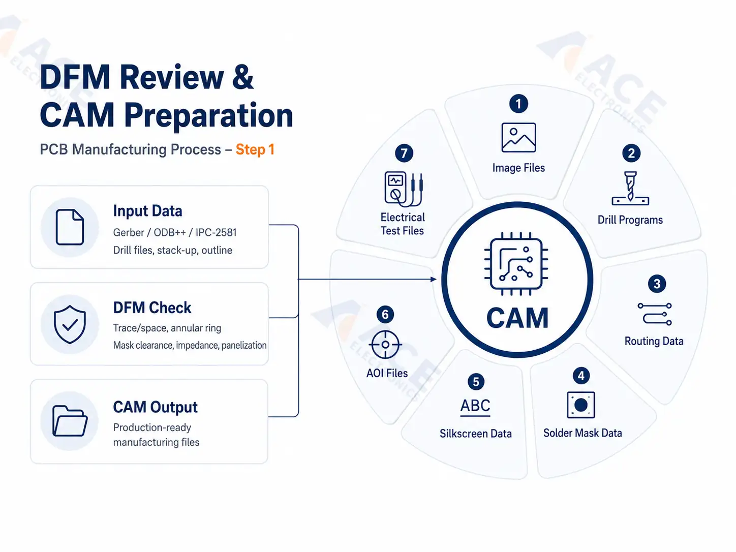 DFM review and engineering data preparation help convert PCB design files into production-ready manufacturing data.
2. Panelization and Tooling Preparation
CAM engineers prepare the design data for manufacturing equipment. They may add tooling holes, fiducials, impedance coupons, test coupons, panel rails, thieving copper, production markings, and process allowances.
Panelization defines how multiple boards are arranged on a production panel. For assembly, the panel needs suitable fiducials, stable rails, and a breakaway method that does not damage components or board edges. Poor panelization can create handling issues during SMT placement, reflow, depaneling, or enclosure assembly.
3. Inner Layer Imaging
For multilayer boards, the inner copper layers are processed before lamination. A photosensitive dry film is applied to the copper-clad laminate, and the circuit pattern is transferred by UV exposure through a phototool or by laser direct imaging.
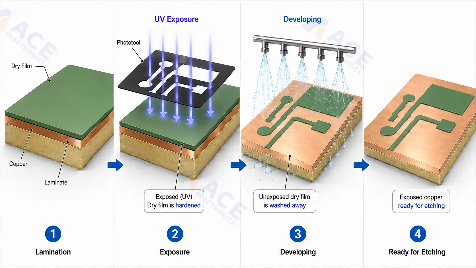 Inner layer imaging transfers the circuit pattern onto the copper surface before etching.
During developing, the UV-hardened dry film stays on the copper, while the unexposed film is washed away. The remaining dry film protects the copper areas that will become traces, pads, or planes. The uncovered copper is then exposed for etching.
Fine traces, tight spacing, and controlled impedance structures depend on accurate image transfer, clean developing, and stable exposure control.
 Photoresist protects selected copper areas during exposure, developing, etching, and resist stripping.
4. Inner Layer Etching and Photoresist Stripping
Etching removes unwanted copper from the inner layers. The remaining copper forms the circuits that will later be buried inside the multilayer board.
 Inner layer etching removes unwanted copper, while photoresist stripping prepares the copper pattern for inspection and bonding.
Etching must be controlled carefully. Over-etching can narrow traces and affect impedance. Under-etching can leave unwanted copper and create shorts. After etching, the remaining photoresist is stripped so the copper pattern can be inspected and prepared for later bonding.
5. AOI for Inner Layers
Automated optical inspection checks the inner layers before they are laminated. This step helps find opens, shorts, copper residues, nicks, spacing violations, and other pattern defects.
Inner layer AOI is important because buried defects are difficult to repair after lamination. For multilayer boards, inspection before pressing reduces the chance of hidden failures in later electrical testing.
6. Roughening Copper and Punching Alignment Holes
After etching and inspection, two things happen to the inner layers before they are pressed together:
-
Punching alignment holes — Small holes are punched through each layer so they can be stacked and aligned precisely during lamination. Misalignment causes vias to miss pads and ruins controlled impedance.
-
Roughening the copper surface — The smooth copper is chemically roughened (often with oxide treatment) so the prepreg can grip it better during hot pressing. Smooth copper bonds poorly and can delaminate.
7. Lay-up and Lamination
During lamination, inner cores, prepreg, copper foil, and other stack-up materials are aligned and pressed together under heat and pressure. The result is a solid multilayer panel.
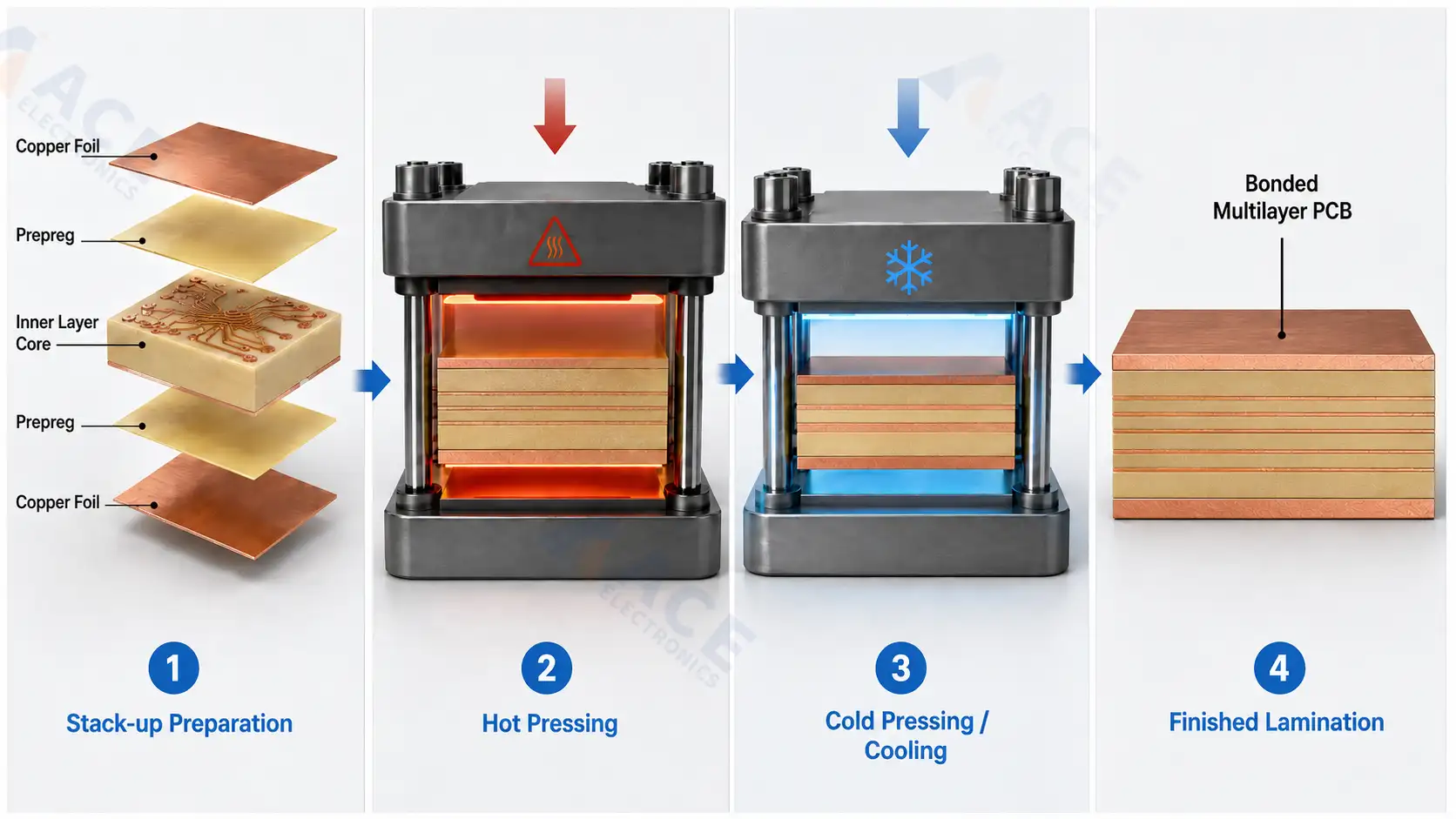 Lay-up and lamination bond cores, prepreg, and copper foil into a solid multilayer PCB panel.
Prepreg flows and cures during pressing, bonding the layers and filling gaps around copper features. Stack-up choices affect board thickness, impedance, dielectric spacing, copper balance, thermal performance, and warpage. Buyers should confirm the stack-up early when the board includes controlled impedance, high-speed signals, thick copper, high layer count, or strict thickness tolerance.
8. Drilling
After lamination, the panel is drilled for vias, component holes, mounting holes, and slots.
| Drill Type | Best For | Limit |
|---|---|---|
| Mechanical (CNC) | Through-holes, vias | Down to ~0.2 mm |
| Laser | Microvias, blind vias | Under ~0.15 mm, not through full panel |
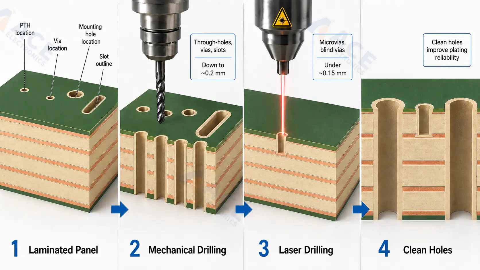 PCB drilling creates vias, component holes, mounting holes, and slots before hole cleaning and copper deposition.
Rough holes, burrs, or smeared resin make the next cleaning and plating step unreliable. Clean holes produce stronger plated vias.
If the same order will continue to PCB assembly, the buyer should also prepare the BOM, pick-and-place file, assembly drawing, polarity notes, approved substitutions, and test instructions. For a practical file checklist, see our guide to Gerber, BOM, pick-and-place, and other PCB assembly files.
9. Hole Cleaning and First Copper Coating
Drilling smears resin across the hole walls and leaves them nonconductive. The factory first cleans the holes and roughens the walls, then applies a very thin layer of copper through a chemical process.
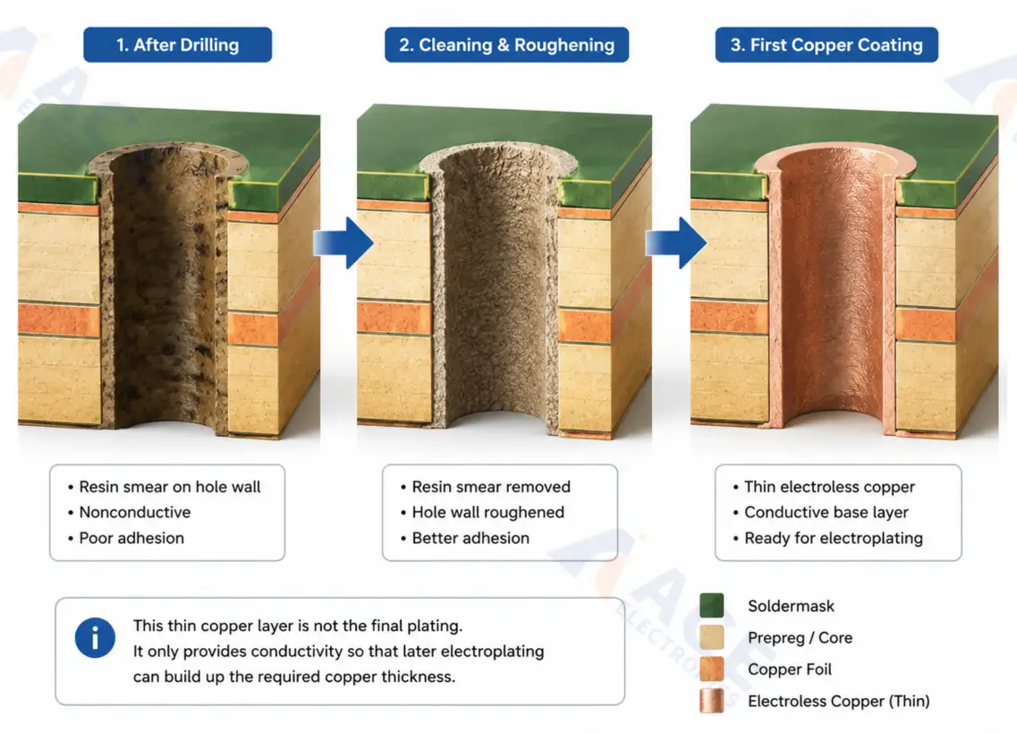 Hole cleaning removes drilling residue, and the first copper coating makes the hole walls conductive for later electroplating.
This thin copper coating is not the final plating. It is only a conductive base so that later electroplating can build real copper thickness inside the holes. Voids, poor hole cleaning, or weak adhesion at this stage can create via reliability problems, especially in high aspect ratio holes.
10. Outer Layer Dry Film Imaging
The outer layers receive dry film photoresist, then the outer circuit image is exposed and developed. Unlike inner-layer processing, the exposed outer-layer copper often defines where additional copper will be plated.
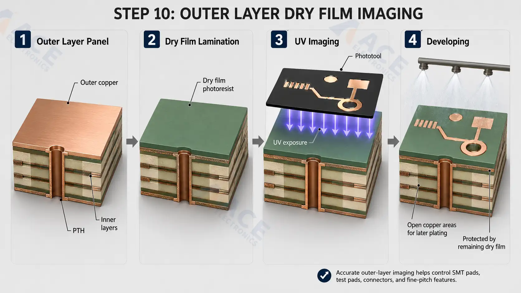 Outer layer dry film imaging defines the areas that will receive additional copper plating.
Outer layer accuracy matters for SMT pads, fine-pitch components, test pads, connectors, and RF or high-speed features. Pad geometry variation can affect solder paste printing, placement, inspection, and rework.
11. Copper Electroplating and Tin Plating
Copper electroplating adds more copper to the hole walls and exposed outer-layer circuit areas.
Before plating, the panel is cleaned and activated. Then the PCB panel is placed in an electrolytic copper bath, where it works as the cathode. Because the drilled holes already have a thin conductive electroless copper layer, copper can now be plated onto the inside of the holes.
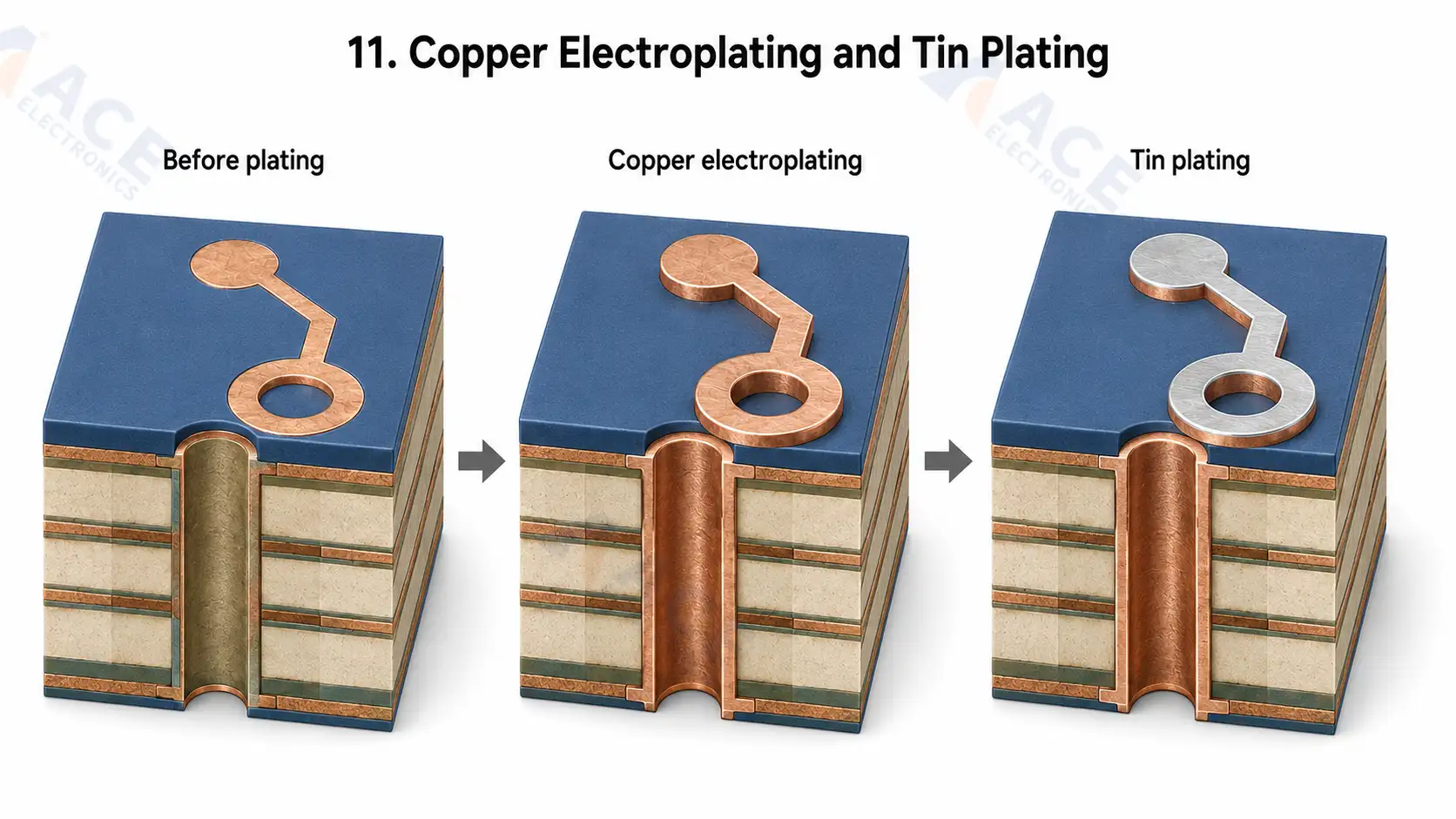 Copper electroplating increases copper thickness in holes and exposed circuit areas, while tin plating protects the circuit image before etching.
This step makes the plated through holes thicker and stronger. It also creates reliable electrical connections between PCB layers.
Tin is often plated over the copper circuit image as an etch resist. It protects the copper features that should remain during the final outer-layer etch.
For high-current boards or reliability-critical boards, the required copper thickness should be clearly stated in the fabrication notes.
12. Outer Layer Strip-Etch-Strip (SES)
After pattern plating, the outer layers go through three consecutive steps to form the final circuit. The cross-sections below show what happens at each stage.
Step 1: Strip photoresist
The dry film is dissolved and washed away. This exposes the unwanted copper that was protected underneath, while the tin layer still covers the circuit traces and pads.
Step 2: Etch exposed copper
Chemical etchant removes the exposed copper. The tin layer acts as a shield — the copper underneath the tin stays intact. This step defines the final trace width and spacing.
Step 3: Strip tin
The tin shield is chemically removed, leaving only the finished copper traces, pads, and plated holes.
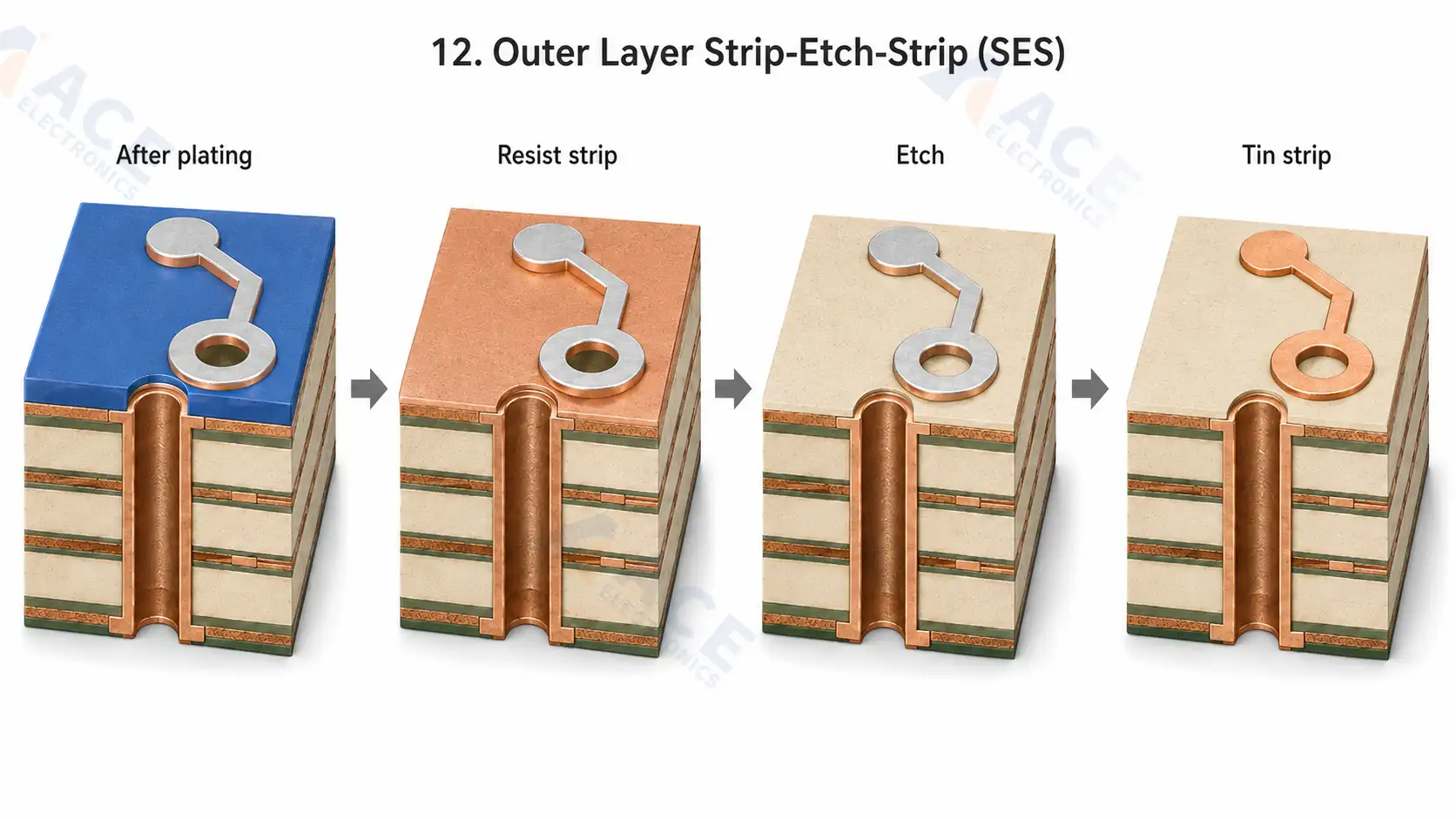 The outer layer strip-etch-strip process removes dry film, etches exposed copper, and strips tin to form the final outer-layer circuit pattern.
What the layers look like at each stage:
| Stage | Top surface | Cross-section detail |
|---|---|---|
| After plating (before SES) | Tin covers circuit areas; photoresist covers unwanted copper | Electrolytic copper + tin on traces; electroless copper base under photoresist |
| After resist strip | Tin still on traces; bare copper exposed everywhere else | Photoresist gone; unwanted copper now exposed for etching |
| After etch | Tin still on traces; unwanted copper removed down to laminate | Only tin-protected copper remains; laminate base visible |
| After tin strip | Clean copper traces and pads exposed | Final circuit pattern ready for solder mask |
This group of steps controls final trace width, spacing, pad shape, and copper residues. Poor control can create shorts, opens, narrow traces, solderability problems, or inspection rejects.
13. Solder Mask Application
Solder mask is the green (or other color) coating that covers most of the board. It protects copper traces from oxidation and short circuits, and it control where solder can and cannot stick.
Most boards use LPI (liquid photo imageable) solder mask. The process works like this:
- Coating — Liquid mask is rolled or sprayed over the entire board surface.
- Imaging — A phototool blocks the pad areas. UV light hardens the mask everywhere else.
- Developing — Unhardened mask over the pads is washed away, exposing the copper.
- Curing — Heat hardens the remaining mask so it bonds permanently to the board.
Solder mask registration directly affects assembly. If the mask opening is off-center or too small, solder paste cannot deposit properly. If the mask opening is too large or misaligned, solder can bridge between tight-pitch pads. BGAs, QFNs, and 0201/01005 passives need precise mask openings and enough solder mask dams between adjacent pads.
14. Surface Finish
Copper pads oxidize quickly in air. The surface finish is a protective coating that keeps pads solderable until assembly.
Common finishes and when to use them:
| Finish | What It Is | Best For | Watch Out For |
|---|---|---|---|
| HASL | Dip in molten solder, blow off excess with hot air | Low-cost, general-purpose boards | Uneven surface; not for fine-pitch or BGAs |
| Lead-free HASL | Same process, lead-free solder alloy | RoHS-compliant general boards | Same planarity issues as tin-lead HASL |
| ENIG | Electroless nickel + thin gold layer | Fine-pitch, BGAs, flat pads, long shelf life | Higher cost; occasional "black pad" defect |
| ENEPIG | Nickel + palladium + gold | Wire bonding, high-reliability, long shelf life | Higher cost than ENIG |
| Immersion silver (ImAg) | Thin silver layer on copper | Fine-pitch, RoHS, good planarity | Tarnishes if exposed to sulfur; handle with gloves |
| Immersion tin (ImSn) | Thin tin layer on copper | Fine-pitch, RoHS, press-fit connectors | Tin whisker risk over time |
| OSP | Organic coating | Low-cost, single-sided, short storage | Limited shelf life; rework degrades coating |
| Hard gold | Thick gold over nickel | Edge connectors, high-wear areas | Expensive; not for general soldering |
For a deeper comparison of HASL, ENIG, OSP, immersion silver, immersion tin, and hard gold, see our PCB surface finish selection guide.
Selection checklist:
- Fine-pitch or BGA? → ENIG, immersion silver, or immersion tin
- Long storage before assembly? → ENIG or ENEPIG
- Lowest cost? → OSP or HASL
- Edge connector or wear surface? → Hard gold
- RoHS required? → Avoid tin-lead HASL
For a deeper comparison of HASL, ENIG, OSP, immersion silver, immersion tin, and hard gold, see our PCB surface finish selection guide.
The wrong finish causes solderability problems, rework, or field failures. Confirm the finish early in the design — changing it later may require pad geometry or stencil adjustments.
15. Silkscreen or Legend Printing
Silkscreen adds reference designators, polarity marks, logos, revision marks, connector labels, and other visual information. It supports inspection, assembly, troubleshooting, and field service.
 Silkscreen adds reference designators, polarity marks, revision labels, and other visual markings for assembly and inspection.
Most factories use LPI (liquid photo imageable) ink or direct legend printing:
LPI ink process:
- Coating — White or colored ink is sprayed or rolled over the solder mask surface.
- Imaging — A phototool blocks the text and symbol areas. UV light hardens the ink everywhere else, or vice versa depending on the ink type.
- Developing — Unhardened ink is washed away, leaving the legend pattern.
- Curing — Heat hardens the ink permanently.
Direct legend printing:
- Printing — An inkjet printer deposits UV-curable ink directly onto the board surface, no phototool needed.
- Curing — UV light instantly hardens the ink.
Direct printing is faster for prototypes and small batches. LPI ink is more durable for high-volume production.
Silkscreen should not overlap pads or critical solderable areas. Ink on pads blocks solder wetting and can cause open joints.
16. Cutting the Board Outline
The factory cuts the panel into individual boards using one of three methods:
| Method | How It Works | Best For |
|---|---|---|
| Routing | CNC mill follows the board outline | Complex shapes, internal slots, tight tolerances |
| V-scoring | V-shaped groove scored across the panel; boards snap apart | Straight-line separation, high-volume rectangular boards |
| Punching | Die punch cuts the outline in one stroke | Simple shapes, very high volume |
Buyers should define the outline, slots, castellations, and edge plating in the fabrication drawing. Tight tolerances matter for connector fit and enclosure assembly.
17. Electrical Testing
Electrical testing verifies that every connection on the bare board matches the design netlist. It catches opens, shorts, and wrong connections before components are mounted.
Two common methods:
| Method | How It Works | Best For | Limitations |
|---|---|---|---|
| Flying probe | Moving probes contact test pads on both sides of the board | Prototypes, small batches, boards without test fixtures | Slower per board; needs accessible test pads |
| Fixture-based (bed of nails) | A custom fixture with spring-loaded pins contacts all test points at once | High-volume production, complex boards | Fixture cost and lead time; needs test point planning |
18. Final Inspection and Packing
Final inspection checks board dimensions, appearance, surface finish, solder mask, silkscreen, board outline, V-cut, routing, revision marking, and packaging. Boards are then packed to reduce handling damage, oxidation, contamination, and mix-ups.
Packing matters when boards will be stored before assembly or shipped to another assembly partner. Moisture protection, labeling, revision control, and clean packaging help reduce avoidable problems before SMT or through-hole assembly begins.
PCB Fabrication vs PCB Assembly vs Turnkey PCBA
PCB fabrication, PCB assembly, and turnkey PCBA are related, but they are not the same service. Clear terminology helps buyers assign the right files, responsibilities, and quality checks to the right supplier.
| Term | Scope | Main output | Best for | Related ACE page |
|---|---|---|---|---|
| PCB fabrication | Manufacturing the bare printed circuit board | Tested bare PCBs | Buyers who need boards before assembly or who already have a separate assembly partner | PCB fabrication |
| PCB assembly | Mounting and soldering components onto the PCB | Assembled PCBAs | Orders where components, placement, soldering, and inspection are needed | PCB assembly and PCBA manufacturing |
| SMT assembly | Placing surface-mount components and reflow soldering | SMT-assembled boards | Dense boards, fine-pitch packages, BGAs, QFNs, passives, ICs | SMT assembly |
| Through-hole assembly | Inserting and soldering leaded components | Boards with through-hole parts installed | Connectors, terminals, transformers, relays, high-mechanical-stress parts | through-hole assembly |
| Turnkey PCBA | Coordinating fabrication, sourcing, assembly, testing, and related production support | Production-ready electronic assemblies | Product teams and purchasing teams that want fewer handoffs across suppliers | PCBA contract manufacturing |
Bare board fabrication ends before components are mounted. PCBA production adds component sourcing, solder paste printing, placement, reflow, through-hole soldering, cleaning when required, inspection, firmware loading, functional testing, coating, and final product assembly.
PCB Manufacturing File Checklist
A complete file package reduces questions before production. It also helps the fabrication team and assembly partner work from the same revision.
| File or data | Needed for fabrication | Needed for assembly | Buyer note |
|---|---|---|---|
| Gerber or ODB++ | Yes | Sometimes | ODB++ or IPC-2581 can reduce layer interpretation issues when supported |
| NC drill file | Yes | Sometimes | Confirm PTH, NPTH, slots, and special hole tolerances |
| Fabrication drawing | Yes | No | Include material, thickness, copper, finish, tolerances, and notes |
| Stack-up drawing | Yes | Sometimes | Required for controlled impedance and multilayer control |
| IPC netlist | Recommended | No | Helps compare design intent with manufacturing output |
| BOM | No | Yes | Needed for sourcing, alternates, and assembly planning |
| Pick-and-place file | No | Yes | Needed for placement coordinates and rotation checks |
| Assembly drawing | No | Yes | Helps confirm polarity, orientation, special handling, and mechanical constraints |
| Test instructions | Sometimes | Yes | Defines electrical, ICT, functional, or customer-specific test expectations |
If buyers plan to place one combined PCB and PCBA order, the file package should be reviewed as one set, not as separate documents passed between suppliers.
How PCB Manufacturing Affects Assembly Quality
Bare board quality affects assembly yield. A board can pass visual inspection and still create assembly problems if the surface finish, solder mask, panelization, flatness, or plated holes are not suitable for the components and process.
| Manufacturing choice | Assembly impact | Buyer note |
|---|---|---|
| Surface finish | Affects solderability, pad flatness, shelf life, and fine-pitch assembly | Match finish to component package, storage time, and soldering process |
| Solder mask registration | Affects solder bridging, exposed copper, and inspection clarity | Important for fine-pitch ICs, BGAs, QFNs, and dense passive areas |
| Panelization | Affects SMT throughput, fiducial recognition, handling, and depaneling | Confirm rails, tooling holes, fiducials, and breakaway method |
| Board flatness | Affects solder paste printing, placement accuracy, and reflow results | Important for thin boards, large panels, BGAs, and heavy copper |
| Drilling and plating | Affects via continuity and through-hole reliability | Confirm aspect ratio, hole tolerance, annular rings, and plating expectations |
| Cleanliness | Affects coating adhesion, leakage risk, and long-term reliability | Especially important before conformal coating |
| Electrical test | Reduces the chance of mounting components on defective boards | Confirm test coverage before assembly starts |
When fabrication and assembly are handled by different suppliers, these details need clear handoff. When they are handled through one coordinated process, DFM feedback, panel design, sourcing questions, assembly planning, and test planning can be reviewed together.
PCB Manufacturing Quality Checks Buyers Should Expect
Buyers should expect quality checks before hidden defects become expensive. Inner-layer defects should be caught before lamination, plating issues before assembly, and open/short defects before components are mounted.
| Quality check | When it happens | What it helps prevent |
|---|---|---|
| CAM and DFM review | Before production release | Unclear files, impossible spacing, drill issues, missing fabrication notes |
| Inner layer AOI | Before lamination | Hidden opens, shorts, copper residues, inner-layer pattern defects |
| Lamination control | During multilayer production | Delamination, thickness variation, stack-up mismatch |
| Drilling and plating inspection | After drilling and plating | Weak vias, poor hole-wall copper, incorrect hole size |
| Solder mask inspection | Before surface finish | Solder bridge risk, exposed copper, mask registration problems |
| Impedance test or coupon | When controlled impedance is required | Signal integrity variation and stack-up mismatch |
| Electrical test | Before shipment or assembly | Opens, shorts, incorrect connectivity |
| Final inspection | Before packing | Dimensional issues, appearance defects, wrong markings, revision mix-ups |
For higher-reliability products, buyers may also request material confirmation, microsection reports, impedance reports, electrical test records, or other documentation defined in the fabrication drawing or purchase requirements.
When Should Buyers Use a Turnkey PCB and PCBA Partner?
Fabrication-only sourcing can work well when the buyer already has a qualified assembly partner, mature documentation, and internal resources to manage supplier handoff. It can also work for bare board validation before the next engineering revision.
Use a turnkey PCB and PCBA partner when the board, components, assembly, testing, and final handling need to be coordinated together. This is common when product teams want fewer handoffs between PCB fabrication, component sourcing, SMT assembly, through-hole assembly, firmware loading, functional testing, coating, and final product assembly.
Supplier coordination becomes more important when one manufacturing choice affects several later steps: surface finish for fine-pitch parts, panelization for SMT efficiency, solder mask clearance for bridging risk, board cleanliness before coating, or test coverage before enclosure assembly.
For projects that need fabrication and assembly support in one flow, ACE Electronics can review the manufacturing files, assembly files, and test expectations before production starts.
Frequently Asked Questions
What should I send to a PCB manufacturer before production starts?
What should I send to a PCB manufacturer before production starts?
You should send Gerber or ODB++ files, NC drill files, a fabrication drawing, stack-up requirements, material requirements, copper weight, board thickness, surface finish, solder mask color, and any impedance or testing requirements. If the order will continue to PCB assembly, also prepare the BOM, pick-and-place file, assembly drawing, polarity notes, and test instructions.
Why does a PCB manufacturer ask DFM questions after I send the files?
Why does a PCB manufacturer ask DFM questions after I send the files?
DFM questions usually mean the factory found something that needs clarification before production. Common issues include tight trace spacing, unclear drill types, missing fabrication notes, insufficient annular rings, undefined stack-up, solder mask clearance problems, or panelization requirements that affect manufacturing.
Is PCB manufacturing the same as PCB fabrication?
Is PCB manufacturing the same as PCB fabrication?
In most buyer and engineering discussions, PCB manufacturing and PCB fabrication both refer to making the bare printed circuit board before components are mounted. PCB assembly is different because it places and solders components onto the bare board to create a PCBA.
Why does PCB manufacturing quality matter if the board will be assembled later?
Why does PCB manufacturing quality matter if the board will be assembled later?
Bare board quality affects assembly because solderability, pad geometry, solder mask registration, board flatness, plated hole quality, panelization, cleanliness, and electrical test results all influence component placement, soldering, inspection, testing, coating, and final product reliability.
Which PCB manufacturing steps affect SMT assembly the most?
Which PCB manufacturing steps affect SMT assembly the most?
The most important steps for SMT assembly are surface finish, solder mask application, outer layer imaging, copper plating, panelization, profiling, and final inspection. These steps affect pad flatness, solder paste printing, fine-pitch placement, solder bridging, fiducial recognition, and depaneling quality.
What causes PCB manufacturing delays?
What causes PCB manufacturing delays?
Common delay causes include incomplete Gerber or drill files, unclear stack-up, missing fabrication drawings, material availability, controlled impedance requirements, special surface finishes, HDI or microvia structures, tight tolerances, engineering questions, and additional testing or documentation requirements.
How do I know whether my PCB needs controlled impedance?
How do I know whether my PCB needs controlled impedance?
Controlled impedance is usually needed when the board carries high-speed digital, RF, microwave, USB, Ethernet, HDMI, PCIe, DDR, or other signal lines where trace geometry and dielectric thickness affect signal performance. If controlled impedance is required, the stack-up, trace width, spacing, dielectric material, and impedance tolerance should be defined before fabrication.
What is the difference between HASL, ENIG, OSP, immersion silver, and immersion tin?
What is the difference between HASL, ENIG, OSP, immersion silver, and immersion tin?
These are surface finishes applied to exposed copper pads. HASL is low-cost but less flat. ENIG is flatter and better for fine-pitch parts and BGAs. OSP is low-cost but has a shorter handling window. Immersion silver offers good planarity but needs careful storage. Immersion tin is flat and solderable but can have shelf-life and whisker concerns.
Should PCB fabrication and PCB assembly be handled by the same supplier?
Should PCB fabrication and PCB assembly be handled by the same supplier?
They do not always need to be handled by the same supplier. Separate suppliers can work if the files, specifications, and handoff are clear. A combined fabrication and assembly partner is more useful when panelization, surface finish, component sourcing, SMT assembly, through-hole assembly, testing, coating, or final product assembly need to be coordinated together.
What quality records should I ask for before boards move to assembly?
What quality records should I ask for before boards move to assembly?
For normal boards, electrical test confirmation and final inspection records are often enough. For controlled impedance, high-reliability, or complex multilayer boards, buyers may also request impedance reports, material confirmation, microsection reports, plating thickness data, solderability confirmation, or other records defined in the fabrication drawing.
Need Fabrication and Assembly Reviewed Together?
If your order needs bare PCB fabrication together with component sourcing, SMT assembly, through-hole assembly, firmware loading, PCBA testing, conformal coating, enclosure assembly, or final product assembly, ACE Electronics can review the manufacturing files and help identify process risks before production starts.