

SMT defects are soldering, placement, or process problems that occur during surface mount PCB assembly. Common SMT defects include solder balls, solder bridging, tombstoning, open solder joints, cold solder joints, component misalignment, solder voids, and solder paste printing defects.
For buyers and hardware teams, SMT defects matter because they affect yield, reliability, test results, rework cost, and delivery risk. A small solder bridge may create an immediate short circuit. A weak solder joint may pass visual inspection but fail later under vibration, heat, or field use.
This guide explains the most common SMT soldering defects, what usually causes them, how they are detected, and what to review with your PCB assembly partner before a prototype or production run.
Common SMT Defects
Common SMT defects include:
- Solder balls
- Solder bridging
- Tombstoning
- Open solder joints
- Insufficient solder
- Excess solder
- Cold solder joints
- Component placement defects
- Missing components
- Component polarity errors
- Lifted leads or lifted components
- Head-in-pillow defects
- Solder voids
- Solder wicking
- Solder cracks
- Non-wetting or de-wetting
- Flux residue or contamination
- Solder paste printing defects
SMT Defects Summary Table
| SMT defect | What it looks like | Common risk | Main process area |
|---|---|---|---|
| Solder balls | Small loose or attached solder spheres near pads | Short circuit, contamination, rework | Solder paste, stencil, reflow |
| Solder bridging | Solder connects adjacent pads or leads | Electrical short | Paste volume, stencil, placement, reflow |
| Tombstoning | One end of a chip component lifts during reflow | Open circuit | Pad design, thermal balance, reflow profile |
| Open solder joint | Pad and lead are not electrically connected | Intermittent or failed circuit | Paste deposit, placement, coplanarity |
| Insufficient solder | Too little solder forms the joint | Weak joint, open circuit, intermittent failure | Stencil, paste release, wetting |
| Excess solder | Too much solder remains around the pad or lead | Bridging, solder balls, poor appearance | Paste volume, stencil, reflow |
| Cold solder joint | Dull, rough, weak solder connection | Weak mechanical and electrical joint | Reflow heat, wetting, contamination |
| Component placement defects | Wrong position, wrong part, missing part, or polarity error | Functional failure, open, short, rework | Pick-and-place, BOM, centroid data, first article inspection |
| Lifted leads or lifted components | A lead or component end is raised from the pad | Open circuit or weak joint | Coplanarity, placement, reflow, board handling |
| Head-in-pillow defect | BGA ball and solder paste touch but do not fully merge | Hidden intermittent connection | BGA coplanarity, oxidation, reflow, X-ray |
| Solder voids | Cavities inside the solder joint | Reduced thermal and mechanical reliability | Reflow, moisture, outgassing |
| Solder wicking | Solder is drawn away from the intended joint area | Insufficient solder or open joint | Pad design, lead finish, thermal imbalance |
| Solder cracks | Cracks form in or around the solder joint | Long-term reliability failure | Thermal cycling, vibration, mechanical stress |
| Flux residue or contamination | Residue remains on the PCB after assembly | Appearance, insulation, corrosion, reliability risk | Flux chemistry, cleaning, process control |
| Non-wetting / de-wetting | Solder does not spread properly on pad or lead | Weak or incomplete joint | Surface finish, oxidation, flux activity |
| Solder paste printing defects | Too much, too little, shifted, or smeared paste | Multiple downstream defects | Stencil printing and SPI |
Why SMT Defects Happen
Most SMT defects are not caused by one single factor. They usually come from a combination of PCB design, solder paste behavior, stencil design, component condition, placement accuracy, reflow profile, and inspection control.
A practical way to diagnose SMT defects is to trace them by process stage:
| Process stage | What can go wrong | Defects it can create |
|---|---|---|
| PCB fabrication and surface finish | Oxidized pads, poor solderability, uneven pad geometry, via-in-pad issues | Non-wetting, opens, tombstoning, solder voids |
| Solder paste storage and handling | Moisture, expired paste, poor warm-up, viscosity change | Solder balls, poor paste release, cold joints |
| Stencil design and printing | Wrong aperture size, stencil misalignment, clogged openings, poor underside cleaning | Bridging, insufficient solder, solder balls, paste smearing |
| Pick-and-place | Incorrect rotation, offset placement, wrong component, missing component, excessive placement pressure | Placement defects, polarity errors, tombstoning, solder balls, opens |
| Reflow soldering | Ramp too fast, poor soak, uneven heat, wrong peak temperature | Tombstoning, cold joints, voids, bridging, incomplete reflow |
| Inspection and testing | Poor inspection coverage, no first article check, missing X-ray for hidden joints | Escaped defects, head-in-pillow defects, polarity errors, field failures |
For a new PCBA order, the best time to reduce SMT defects is before assembly starts. A complete manufacturing package helps the assembly partner review Gerber files, BOM, pick-and-place data, assembly drawings, and test requirements before the first board enters production. See ACE's PCB Assembly Files Guide for the file set typically needed.
Solder Balls
Solder balls are small spheres of solder that appear on the PCB surface after reflow. They may sit near chip components, fine-pitch ICs, pads, or solder mask areas.
Common Causes of Solder Balls
Solder balls are usually caused by excess paste, moisture, stencil contamination, placement pressure, or an aggressive reflow profile.
Common causes include:
- Poor solder paste warm-up or handling
- Moisture in solder paste, PCB, or components
- Excess solder paste volume
- Stencil underside contamination
- Poor stencil aperture design
- Excessive placement pressure
- Rapid reflow ramp rate
- PCB or FPC material moisture before assembly
| Cause | What it means | Prevention |
|---|---|---|
| Poor solder paste warm-up or handling | Paste viscosity becomes unstable before printing | Control storage, warm-up time, and exposure time |
| Moisture in paste, PCB, or components | Moisture expands during reflow and can push solder outward | Bake moisture-sensitive boards or components when required |
| Excess solder paste volume | Too much paste is squeezed out during placement or reflow | Review stencil aperture size and stencil thickness |
| Stencil underside contamination | Residue transfers paste outside the intended pad area | Clean stencil underside at defined intervals |
| Poor stencil aperture design | Paste release or paste volume does not match the pad geometry | Adjust aperture reduction, shape, and stencil thickness |
| Excessive placement pressure | The component body pushes paste under or around the part | Reduce placement force and verify placement height |
| Rapid reflow ramp rate | Solvent and flux outgas too quickly during heating | Use a reflow profile that allows controlled outgassing |
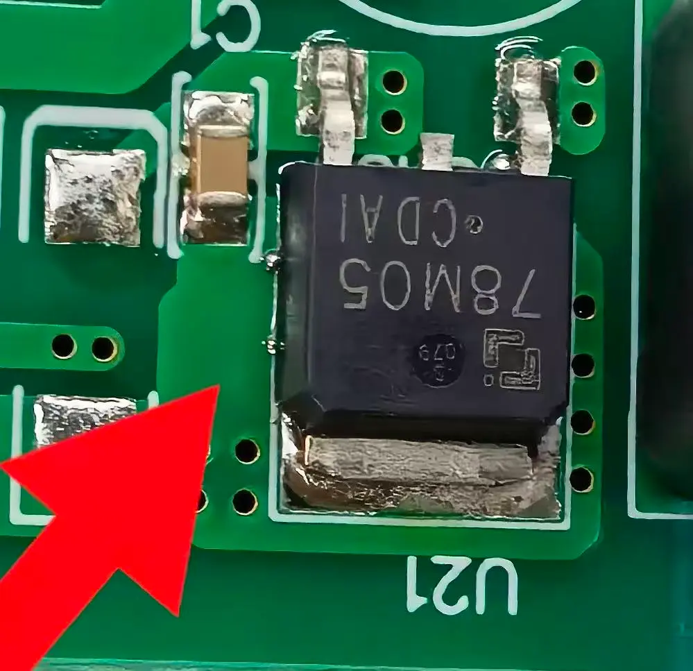
Solder balls are small solder spheres that can appear near SMT pads or component bodies after reflow.
Solder Bridging
Solder bridging happens when solder creates an unintended connection between two adjacent pads, pins, or conductors. It is one of the most serious SMT defects because it can create a direct electrical short.
Common Causes of Solder Bridging
Solder bridging is usually related to excess solder, paste misalignment, placement offset, or not enough separation between solder deposits.
Common causes include:
- Too much solder paste on fine-pitch pads
- Stencil aperture too large for pad spacing
- Stencil misalignment during printing
- Solder paste slump before reflow
- Component placement offset
- Reflow profile causing uncontrolled solder flow
- Pad design that does not leave enough solder mask clearance control
| Cause | Prevention |
|---|---|
| Too much solder paste on fine-pitch pads | Use correct stencil aperture reduction for fine-pitch ICs |
| Stencil aperture too large for pad spacing | Review aperture width, length, and area ratio during DFM |
| Stencil misalignment during printing | Keep printer setup stable and verify alignment before production |
| Solder paste slump before reflow | Control paste handling, room conditions, and open time |
| Component placement offset | Confirm pick-and-place accuracy before reflow |
| Reflow profile causing uncontrolled solder flow | Tune ramp, soak, and peak temperature for the board design |
| Hidden bridge risk under leadless packages | Use X-ray for BGA, QFN, LGA, and other hidden joints |
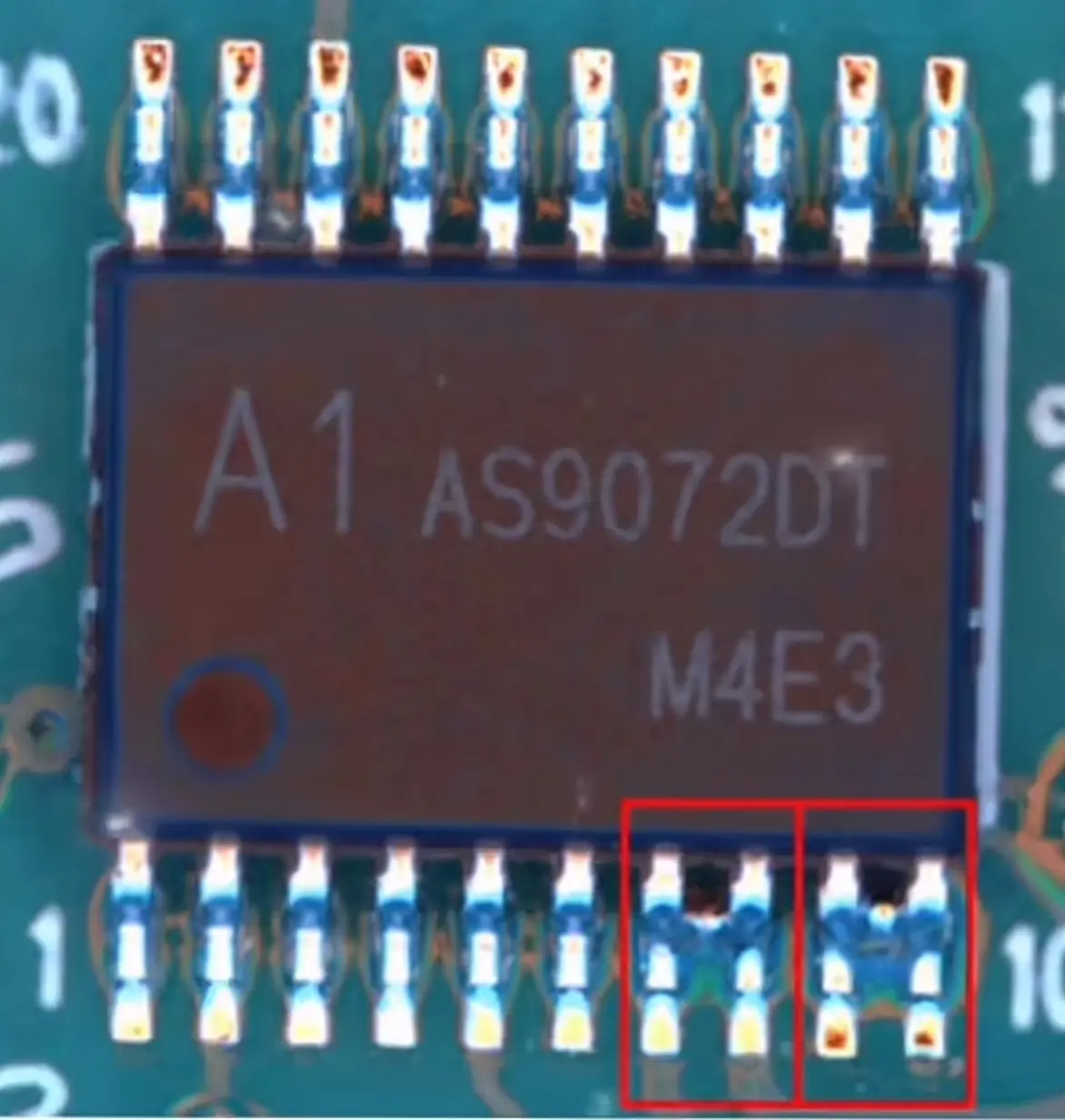
Solder bridging creates an unintended conductive path between adjacent pads, leads, or conductors.
For projects with fine-pitch parts, BGA, QFN, or high-density SMT placement, review ACE's SMT Assembly capabilities and inspection controls.
Tombstoning in SMT
Tombstoning happens when one end of a small passive component lifts during reflow. The component stands upright or partially upright, leaving one side disconnected.
Common Causes of Tombstoning
Tombstoning is usually caused by unbalanced wetting forces. One side of the component reaches molten solder and pulls earlier than the other side.
Typical causes include:
- Unequal pad sizes
- Uneven copper connection to each pad
- One pad connected to a large copper area or via while the other is not
- Unbalanced solder paste volume
- Component not centered on both pads
- Uneven heating across the PCB
- Reflow soak not long enough to balance temperature
- Very small chip components such as 0402, 0201, or 01005
| Cause | Prevention |
|---|---|
| Unequal pad sizes | Keep pad geometry balanced for two-terminal chip components |
| Uneven copper connection to each pad | Avoid heavy copper imbalance between the two pads |
| Via or large copper area on one side only | Avoid via-in-pad unless the via is properly filled or plugged |
| Unbalanced solder paste volume | Use consistent paste volume on both pads |
| Component not centered on both pads | Improve placement centering and verify pick-and-place data |
| Uneven heating across the PCB | Use a reflow profile with enough soak time for thermal balance |
| Very small chip components | Review 0402, 0201, and 01005 packages during DFM before production |
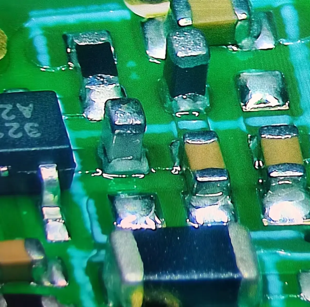
Tombstoning happens when one end of a chip component lifts during reflow, leaving an open connection.
ACE provides PCB design and DFM support for layout-related manufacturability issues such as pad balance, fine-pitch spacing, and assembly risk review.
Open Solder Joints and Insufficient Solder
An open solder joint occurs when the component terminal and PCB pad are not properly connected. Insufficient solder may appear as a weak or incomplete fillet, while a full open may show no reliable electrical path.
Common Causes
Open solder joints and insufficient solder usually come from missing paste, poor paste release, pad contamination, placement offset, or incomplete wetting during reflow.
Common causes include:
- Too little solder paste printed on the pad
- Clogged stencil aperture
- Poor paste release from the stencil
- Component lead or terminal coplanarity problem
- Placement offset
- Pad oxidation or contamination
- PCB surface finish issue
- Reflow temperature too low for complete wetting
- Solder wicking away from the intended joint area
- Via-in-pad pulling solder away from the joint
| Cause | Prevention |
|---|---|
| Too little solder paste printed on the pad | Check stencil aperture ratio and area ratio |
| Clogged stencil aperture | Clean stencil openings regularly |
| Poor paste release from the stencil | Review stencil thickness, aperture geometry, and paste condition |
| Component coplanarity problem | Review component coplanarity for leaded packages |
| Placement offset | Confirm placement accuracy and component package match |
| Pad oxidation or contamination | Confirm surface finish and pad cleanliness |
| Reflow temperature too low | Verify the measured board-level reflow profile |
| Solder wicking away from the joint | Review pad design, lead finish, and local thermal balance |
| Via-in-pad pulling solder away | Avoid untreated via-in-pad under solderable pads |
For assemblies that require end-of-line verification, ACE supports firmware loading and functional testing to confirm that the completed PCBA works as intended.
Cold Solder Joints
A cold solder joint is a weak joint formed when solder does not fully melt, flow, or bond properly. It may look dull, grainy, rough, or irregular.
Common Causes
Cold solder joints are usually caused by insufficient heat, poor wetting, oxidation, contamination, or solder paste that no longer performs correctly.
Common causes include:
- Insufficient heat during reflow
- Incorrect peak temperature
- Poor thermal transfer to large pads or high-mass areas
- Contaminated pads or terminals
- Oxidized component leads
- Expired or poorly handled solder paste
- Flux activity exhausted before proper wetting
| Cause | Prevention |
|---|---|
| Insufficient heat during reflow | Confirm the profile using board-level temperature measurement |
| Incorrect peak temperature | Check the required solder alloy and paste datasheet |
| Poor thermal transfer to high-mass areas | Profile the most thermally demanding areas of the PCB |
| Contaminated pads or terminals | Review PCB surface finish, cleanliness, and component condition |
| Oxidized component leads | Control component storage and check solderability risk |
| Expired or poorly handled solder paste | Control paste storage, warm-up, and exposure time |
| Flux activity exhausted before wetting | Use a suitable profile and paste for the process window |
Non-Wetting and De-Wetting
Non-wetting happens when solder does not spread properly across the pad or component termination. De-wetting happens when solder initially wets the surface but then pulls back, leaving exposed metal or an irregular solder shape.
Common causes include oxidation, poor PCB surface finish, contamination, insufficient flux activity, incompatible solder paste, or an unsuitable reflow profile.
| Cause | Prevention |
|---|---|
| Oxidized pads or component terminals | Control PCB and component storage conditions |
| Poor PCB surface finish | Confirm surface finish quality and solderability before assembly |
| Contamination on pads or leads | Improve handling, cleaning, and process cleanliness |
| Insufficient flux activity | Use suitable solder paste for the process and surface finish |
| Reflow profile outside the paste window | Verify the measured reflow profile on a representative board |
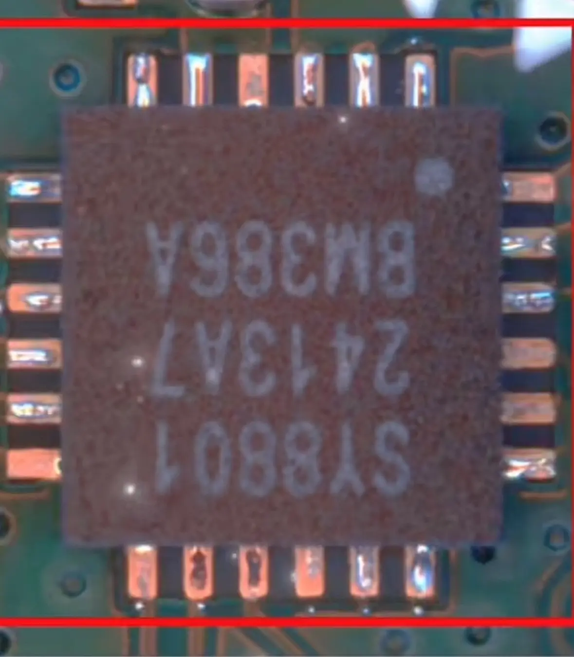
Non-wetting leaves an incomplete solder bond because solder does not spread correctly on the pad or termination.
Component Placement Defects
Component placement defects include misaligned parts, wrong component values, missing components, polarity errors, and lifted leads or lifted components. These defects may cause opens, shorts, incorrect circuit behavior, or complete functional failure.
Common Causes
Placement defects are usually caused by file errors, BOM mismatch, feeder setup mistakes, package mismatch, poor fiducial recognition, placement calibration issues, or shifted paste deposits.
Common causes include:
- Incorrect pick-and-place data
- Wrong component rotation in the centroid file
- Wrong component loaded into the feeder
- Component value or package mismatch in the BOM
- Missing component during placement
- Polarity or orientation error on diodes, LEDs, electrolytic capacitors, connectors, or ICs
- Lifted lead or lifted component caused by coplanarity, handling, or reflow movement
- Poor fiducial recognition
- Placement machine calibration issue
- Excessive vibration before reflow
- Paste deposit shifted from pad location
| Cause | Prevention |
|---|---|
| Incorrect pick-and-place data | Provide accurate centroid data and verify coordinates |
| Wrong component rotation | Include assembly drawings for polarity and orientation details |
| Wrong component loaded into the feeder | Use barcode control, feeder verification, and first article inspection |
| Component value or package mismatch | Confirm BOM manufacturer part numbers, approved alternates, and footprints |
| Missing component during placement | Use AOI and first article inspection before production release |
| Polarity or orientation error | Mark polarity clearly in the assembly drawing and silkscreen when possible |
| Lifted lead or lifted component | Check component coplanarity, placement force, and reflow movement |
| Poor fiducial recognition | Use clear global and local fiducials where needed |
| Placement machine calibration issue | Run first article inspection before production release |
| Excessive vibration before reflow | Control board handling between placement and reflow |
| Paste deposit shifted from pad location | Use SPI and AOI to catch paste and placement offset early |
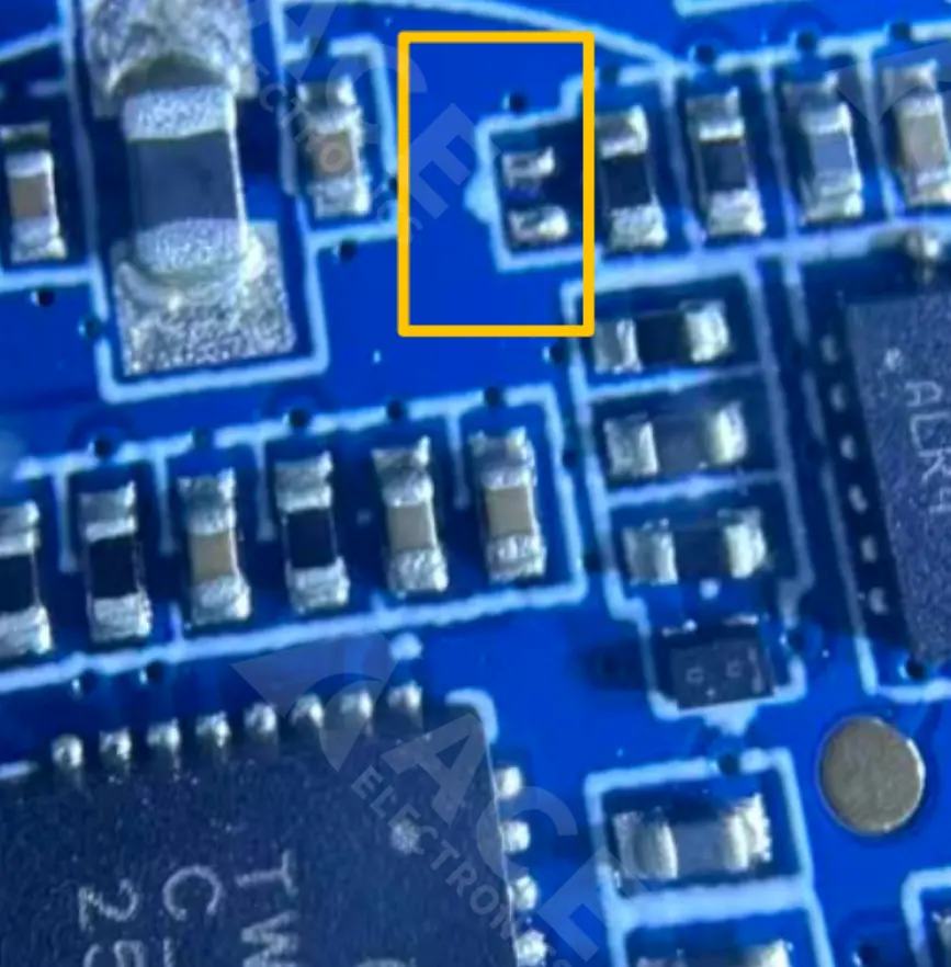
Missing components are usually caught by AOI, first article inspection, or functional testing before shipment.
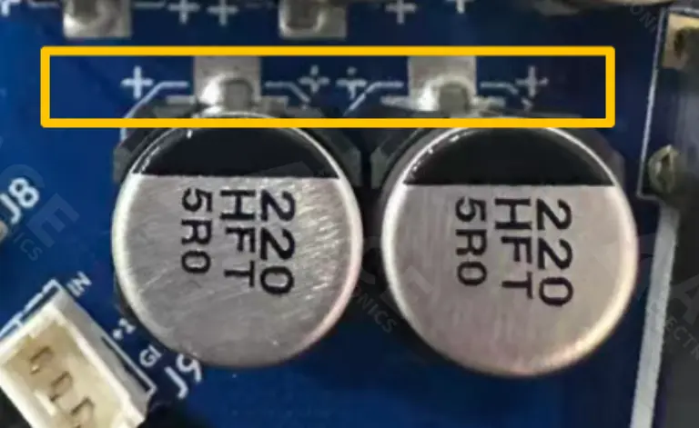
Polarity errors can affect diodes, LEDs, electrolytic capacitors, connectors, ICs, and other orientation-sensitive parts.
For file preparation details, see the PCB Assembly Files Guide.
Head-in-Pillow Defects
A head-in-pillow defect is a hidden BGA soldering defect where the solder ball and solder paste appear to touch but do not fully merge into one reliable solder joint. It may pass a simple visual review because the joint is under the BGA package, but it can create intermittent electrical failure.
Common Causes
Head-in-pillow defects are usually related to BGA ball oxidation, package warpage, poor paste wetting, poor coplanarity, or an unsuitable reflow profile.
Common causes include:
- Oxidized BGA solder balls
- Oxidized or contaminated PCB pads
- BGA package warpage during reflow
- Poor solder paste wetting
- Insufficient paste volume on BGA pads
- Incomplete thermal profile for the BGA area
- Long storage time or poor component handling
| Cause | Prevention |
|---|---|
| Oxidized BGA solder balls | Control component storage and review solderability risk |
| Oxidized or contaminated PCB pads | Confirm surface finish quality and pad cleanliness |
| BGA package warpage during reflow | Review package handling, moisture sensitivity, and reflow profile |
| Poor solder paste wetting | Use suitable paste and verify paste shelf life and exposure time |
| Insufficient paste volume | Check stencil aperture design and SPI data for BGA pads |
| Incomplete thermal profile | Measure the profile near the BGA, not only at the board edge |
| Hidden joint risk | Use X-ray inspection and functional testing for BGA assemblies |
Solder Voids
Solder voids are cavities trapped inside a solder joint. Small voids may be acceptable depending on the product and acceptance class, but excessive voiding can reduce thermal transfer, current capacity, and mechanical reliability.
Where Voids Matter Most
Voids are especially important under:
- BGA solder balls
- QFN thermal pads
- Power components
- LED thermal pads
- High-current joints
- Components exposed to vibration or thermal cycling
Common Causes
Solder voids are usually caused by outgassing, moisture, large paste deposits, poor thermal pad aperture design, or a reflow profile that traps gas inside the joint.
Common causes include:
- Flux outgassing during reflow
- Moisture in PCB material or components
- Large paste deposit with poor gas escape path
- Poor thermal pad aperture design
- Reflow profile not allowing enough outgassing time
- Surface finish or pad contamination
| Cause | Prevention |
|---|---|
| Flux outgassing during reflow | Tune reflow soak and peak profile to allow gas escape |
| Moisture in PCB material or components | Control moisture exposure and bake when required |
| Large paste deposit with poor gas escape path | Use segmented stencil apertures for large thermal pads |
| Poor thermal pad aperture design | Review aperture pattern, coverage ratio, and paste release |
| Reflow profile traps gas inside the joint | Measure the reflow profile on a representative board |
| Surface finish or pad contamination | Confirm pad cleanliness and solderability before assembly |
| Hidden voids under BGA or QFN packages | Use X-ray inspection and define acceptable voiding criteria before production |
ACE's SMT Assembly process includes X-ray inspection for hidden joints such as BGA and QFN packages when required.
Solder Paste Printing Defects
Solder paste printing is one of the most important SMT process stages because paste defects often become solder defects after reflow.
Common Solder Paste Printing Problems
| Paste printing issue | Possible result after reflow |
|---|---|
| Too much paste | Bridging, solder balls, solder beading |
| Too little paste | Open joints, weak joints, insufficient solder |
| Shifted paste | Misalignment, bridging, opens |
| Smeared paste | Solder balls, shorts, contamination |
| Clogged aperture | Missing solder, open joints |
| Poor paste release | Inconsistent solder volume |
| Stencil underside residue | Solder balls and bridging |
What to Check
Buyers could ask whether the assembly partner uses controls such as:
- Stencil design review
- Solder paste storage control
- Printer setup verification
- Stencil cleaning schedule
- 3D SPI after solder paste printing
- First article inspection for new products
- Reflow profile measurement for representative boards
Residue, Contamination, and Solder Cracks
Some SMT defects are less about immediate assembly yield and more about long-term reliability. Flux residue, ionic contamination, and solder cracks can affect insulation resistance, corrosion risk, field reliability, and customer acceptance.
| Issue | What it means | Prevention or control |
|---|---|---|
| Flux residue | Visible or invisible residue remains after soldering | Match flux chemistry to cleaning requirements and acceptance standards |
| Ionic contamination | Conductive residues remain on the PCB surface | Use proper cleaning control and cleanliness testing when required |
| Surface contamination | Oil, dust, oxidation, or process residue affects solderability | Control PCB handling, storage, and process cleanliness |
| Solder cracks | Cracks form in or around the solder joint | Review thermal cycling, vibration, board support, and component stress |
| Mechanical stress after assembly | Boards are bent, fastened, or handled in a way that stresses joints | Review panelization, depaneling, enclosure assembly, and final product assembly |
These issues are especially important for industrial, automotive-adjacent, outdoor, high-humidity, high-vibration, or long-life products. They should be reviewed together with testing requirements, coating requirements, and enclosure-level assembly conditions.
For boards exposed to moisture, chemicals, dust, or outdoor environments, review whether conformal coating is needed after assembly.
How SMT Defects Are Detected
No single inspection method catches every SMT defect. A reliable inspection plan usually combines paste inspection, optical inspection, X-ray, and electrical or functional testing.
| Inspection method | Best for detecting | Limitation |
|---|---|---|
| 3D SPI | Paste height, volume, area, offset, bridging risk | Before components are placed only |
| AOI | Missing parts, polarity, visible bridges, tombstoning, misalignment | Cannot see hidden BGA/QFN joints |
| X-ray | BGA bridges, voids, head-in-pillow risk, QFN joints | Not needed for every simple PCBA |
| First Article Inspection | BOM match, orientation, placement, value checks | Must be done before production release |
| ICT | Opens, shorts, component value issues | Requires test access and fixture planning |
| Functional testing | Confirms board-level operation | Test coverage depends on customer procedure |
For turnkey PCBA projects, inspection should match the risk level of the product. A simple sensor board may need AOI and functional testing. A high-density industrial controller with BGA, fine-pitch ICs, and loaded firmware may need SPI, AOI, X-ray, firmware loading, and functional testing.
What Buyers Should Send Before SMT Assembly
A complete and consistent file package reduces avoidable SMT defects. Before requesting a quote or starting a production run, prepare:
- Gerber and drill files
- BOM with manufacturer part numbers and approved alternates
- Pick-and-place file
- Assembly drawing with polarity and orientation details
- PCB stackup and surface finish notes
- Special soldering requirements
- Test procedure and pass/fail criteria
- Firmware files if firmware loading is required
- Revision notes showing the approved file set
For turnkey projects, ACE can combine PCB fabrication, component sourcing, SMT assembly, inspection, testing, coating, and final product assembly under one workflow.
SMT Defects Troubleshooting Checklist
Use this checklist when reviewing SMT defects with an assembly partner.
| Question | Why it matters |
|---|---|
| Is the defect visible before or after reflow? | Separates printing/placement issues from reflow issues |
| Is the defect repeated at the same location? | Points to footprint, stencil, or local thermal design |
| Does it affect one component package or many packages? | Helps isolate component, paste, or global process causes |
| Was SPI data checked? | Confirms whether paste volume or offset started the issue |
| Was the reflow profile measured on a representative board? | Confirms actual board temperature, not only oven settings |
| Are the affected pads connected to uneven copper areas? | Important for tombstoning and wetting imbalance |
| Are components moisture-sensitive? | Helps explain voids, solder balls, and package damage |
| Is the issue visible by AOI or only by X-ray/test? | Determines inspection coverage needed |
| Did the issue appear after a revision change? | Points to file, BOM, footprint, or process change |
| Is rework acceptable for this product? | Some high-reliability products need stricter prevention rather than repair |
When to Involve DFM Review
DFM review is useful when SMT defects are linked to design or documentation rather than only line setup. Involve DFM review when the design includes:
- 01005, 0201, or dense 0402 passives
- Fine-pitch ICs or connectors
- BGA, QFN, LGA, or thermal-pad packages
- Via-in-pad
- Large copper imbalance around small components
- Mixed heavy and small components on the same side
- Tight solder mask clearances
- Double-sided SMT with heavy components
- High-current or high-temperature operation
- Functional test or firmware loading requirements
A good assembly partner should not only report defects after they happen. They should also review risk points before assembly, define inspection coverage, and communicate changes clearly before a production run.
Working With an Assembly Partner on SMT Defect Prevention
When comparing PCB assembly suppliers, do not only ask whether they can place the smallest component. Ask how they control the process.
Useful questions include:
- Do you review stencil aperture design before SMT assembly?
- Do you use 3D SPI after solder paste printing?
- How do you control solder paste storage and exposure time?
- How is the reflow profile created and verified?
- When do you use X-ray inspection?
- Do you run first article inspection before production?
- Can you provide inspection feedback if a defect is linked to PCB layout?
- Can you support firmware loading and functional testing after assembly?
ACE Electronics supports turnkey PCBA orders from fabrication and component sourcing through SMT assembly, through-hole assembly, testing, coating, and final product assembly. If your team is preparing a new PCBA order and wants a manufacturability review before production, send your Gerber files, BOM, pick-and-place file, and assembly notes for review.
Frequently Asked Questions
What are common SMT defects?
What are common SMT defects?
Common SMT defects include solder balls, solder bridging, tombstoning, open solder joints, cold solder joints, insufficient solder, component misalignment, solder voids, non-wetting, de-wetting, and solder paste printing defects. Many of these defects start during solder paste printing or placement and become visible after reflow.
What causes solder balls in SMT assembly?
What causes solder balls in SMT assembly?
Solder balls are commonly caused by excess solder paste, moisture in solder paste or PCB material, stencil underside contamination, poor paste release, high placement pressure, or an aggressive reflow ramp. Prevention usually requires solder paste control, stencil cleaning, aperture review, and reflow profile adjustment.
How do you prevent solder bridging in SMT?
How do you prevent solder bridging in SMT?
Solder bridging can be reduced by controlling solder paste volume, using correct stencil aperture design, improving printer alignment, checking paste deposits with SPI, improving placement accuracy, and using a suitable reflow profile. Fine-pitch components should be reviewed carefully during DFM.
What causes tombstoning in SMT?
What causes tombstoning in SMT?
Tombstoning is caused by unbalanced wetting forces during reflow. Common reasons include unequal pad design, uneven copper connections, thermal imbalance, inconsistent paste volume, placement offset, or uneven heating. Small chip components such as 0402, 0201, and 01005 are more sensitive to tombstoning.
What causes cold solder joints in SMT?
What causes cold solder joints in SMT?
Cold solder joints are usually caused by insufficient heat, poor wetting, contamination, oxidation, incorrect reflow profile, expired solder paste, or thermal imbalance on the PCB. They may appear dull, rough, grainy, or weak compared with a properly formed solder joint.
How does solder paste affect SMT defects?
How does solder paste affect SMT defects?
Solder paste affects many SMT defects because it controls solder volume, placement tack, wetting, and joint formation. Too much paste can cause bridging and solder balls. Too little paste can cause open joints. Poorly stored or expired paste can cause weak wetting, voids, and inconsistent results.
How are SMT defects detected during PCB assembly?
How are SMT defects detected during PCB assembly?
SMT defects are detected using a combination of 3D SPI, AOI, X-ray inspection, first article inspection, ICT, and functional testing. SPI checks solder paste before placement. AOI checks visible assembly defects. X-ray is used for hidden solder joints such as BGA and QFN packages. Functional testing confirms that the finished PCBA works as required.