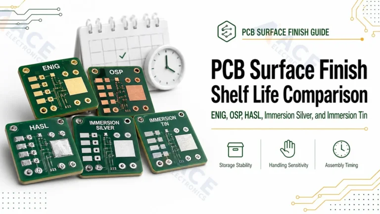
ENIG is one of the most common PCB surface finishes for BGA, QFN, fine-pitch ICs, HDI boards, and high-reliability PCB assembly.
But if you are a PCB designer, ENIG should not be treated as a vague "gold finish" note in your fabrication drawing.
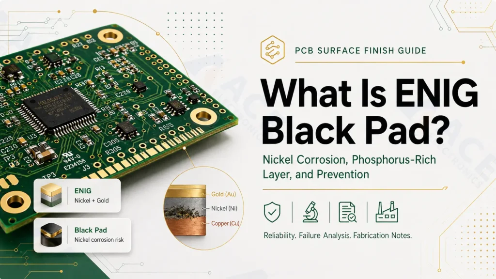
ENIG uses an electroless nickel layer under a thin immersion gold layer. If the plating process is not controlled well, the nickel surface can be corroded before assembly. This can create a defect commonly called black pad.
Black pad may appear later as weak solder joints, brittle fracture, BGA opens, intermittent failure, or poor reliability after thermal cycling.
The related term phosphorus-rich layer is also important. It describes a phosphorus-enriched region at the solder joint interface. A thin phosphorus-rich layer can be part of the normal reaction between solder and electroless nickel. But if it becomes excessive, continuous, or linked with nickel corrosion, it can become a weak fracture path.
For PCB designers, the key question is :
Have I specified ENIG clearly enough for this board's assembly and reliability risk?
Before releasing Gerber files for PCB fabrication service, designers should understand where ENIG risk comes from, when it matters, and what should be written in the fabrication notes.
For a basic introduction to the finish itself, read our guide to ENIG PCB surface finish. This article focuses on black pad, phosphorus-rich layers, failure analysis clues, and design-side prevention.
Quick Answer: What Is ENIG Black Pad?
ENIG black pad is a plating-related defect associated with excessive corrosion of the electroless nickel layer during the immersion gold process.
ENIG has two main metallic layers over copper:
| Layer | Function |
|---|---|
| Electroless nickel | Main solderable layer and diffusion barrier over copper |
| Immersion gold | Protects nickel from oxidation before soldering |
During soldering, the thin gold layer dissolves into the solder. The solder joint then forms mainly with the nickel layer underneath.
When black pad occurs, the nickel surface has already been damaged before soldering. The solder joint may still form, but the interface can be weak and brittle.
Simple explanation:
- ENIG is reliable when the plating process is controlled.
- Black pad is not a normal feature of ENIG.
- Black pad is usually linked to nickel corrosion and poor ENIG process control.
- The failure is often hidden until assembly, testing, or field use.
- BGA, QFN, fine-pitch, and high-reliability boards are more sensitive to this risk.
What Is a Phosphorus-Rich Layer?
Electroless nickel in ENIG is normally a nickel-phosphorus deposit.
During soldering, nickel reacts with tin in the solder and forms nickel-tin intermetallic compounds. Phosphorus does not react in the same way. As nickel is consumed, phosphorus may become concentrated near the solder joint interface.
This is called a phosphorus-rich layer.
A thin phosphorus-rich layer is not automatically a failure. The concern is when the layer becomes too thick, too continuous, or connected with nickel corrosion from the ENIG process. In that case, the interface can become brittle and more likely to crack.
For designers, the practical takeaway is:
The phosphorus-rich layer is an interface reliability issue. It matters most when the board uses small solder joints, BGA, fine-pitch packages, high thermal stress, vibration, or long field-life requirements.
Black Pad vs Phosphorus-Rich Layer
Black pad and phosphorus-rich layer are related, but they are not the same thing.
| Issue | What it means | Why designers should care |
|---|---|---|
| Black pad | Nickel corrosion under the gold layer before soldering | Can create weak or brittle solder joints |
| Phosphorus-rich layer | Phosphorus-enriched region at the solder interface | Can become a fracture path if excessive |
| Nickel corrosion | Damage to the nickel layer during ENIG plating | Often linked to black pad failure |
| Brittle fracture | Solder joint breaks at or near the ENIG interface | Can cause hidden BGA or fine-pitch failures |
In real failure analysis, these conditions may appear together. A failed solder joint may show nickel corrosion, abnormal intermetallic formation, a dark or rough nickel surface, and a phosphorus-rich interface.
That is why black pad should not be treated as only a cosmetic issue. It is a solder joint reliability problem.
Why This Matters During PCB Design
PCB designers do not control the plating bath. But designers do control the fabrication drawing, finish selection, reliability assumptions, and release notes.
That means you can reduce risk before production starts.
Black pad risk matters more when the design includes:
- BGA packages
- QFN, LGA, CSP, or fine-pitch ICs
- HDI stackups
- Small solder joints
- Large thermal pads
- High I/O count components
- Lead-free reflow
- Double-sided SMT
- Long product service life
- Vibration, drop, or thermal cycling requirements
- Medical, automotive, aerospace, industrial, or communication applications
For a simple board with large SMT pads, ENIG black pad risk may be less critical. For a dense BGA board, the same issue can cause expensive validation failure or field returns.
If your design uses BGA or fine-pitch packages, also read our guide to the best PCB surface finish for BGA assembly.
What Causes ENIG Black Pad?
ENIG black pad usually comes from poor control of the ENIG plating process.
The main causes include excessive nickel corrosion, poorly controlled gold deposition, nickel phosphorus instability, contaminated chemistry, weak process monitoring, and poor surface preparation.
1. Excessive Nickel Corrosion During Immersion Gold
Immersion gold is a displacement reaction. Gold deposits while nickel is partially dissolved.
If the gold bath is too aggressive, the dwell time is too long, or the chemistry is not controlled properly, the nickel layer can be over-corroded. This creates a damaged nickel surface under the gold layer.
After assembly, the solder joint may fracture at this weakened interface.
2. Poor Gold Thickness Control
Gold thickness matters.
Too little gold may not protect the nickel surface well enough before assembly. Too much immersion gold can increase the displacement reaction and raise the chance of nickel corrosion.
This is why designers should not write only "gold finish" in the fabrication notes. The finish should be specified as ENIG with an applicable standard and controlled thickness range.
3. Nickel Phosphorus Process Problems
The electroless nickel layer contains phosphorus. The phosphorus level affects corrosion behavior and solder joint formation.
If the nickel-phosphorus deposit is outside the supplier's controlled process window, the surface may become more vulnerable to corrosion or may form a weaker solder joint interface.
Designers do not need to manage the chemistry, but they should specify a recognized ENIG requirement and use a PCB fabricator with proven ENIG process control.
4. Plating Bath Contamination or Aging Chemistry
ENIG is a chemical process. Bath contamination, incorrect pH, poor replenishment, temperature drift, or aging chemistry can all affect the final finish.
This is why two suppliers can both quote "ENIG" but deliver different reliability results.
The drawing note is important, but supplier process control is just as important.
5. Poor Surface Preparation Before ENIG
Before nickel plating, copper pads must be cleaned and prepared correctly.
Residue, oxidation, solder mask contamination, or poor micro-etching can affect plating uniformity and adhesion. These problems may later show up as solderability or joint reliability issues.
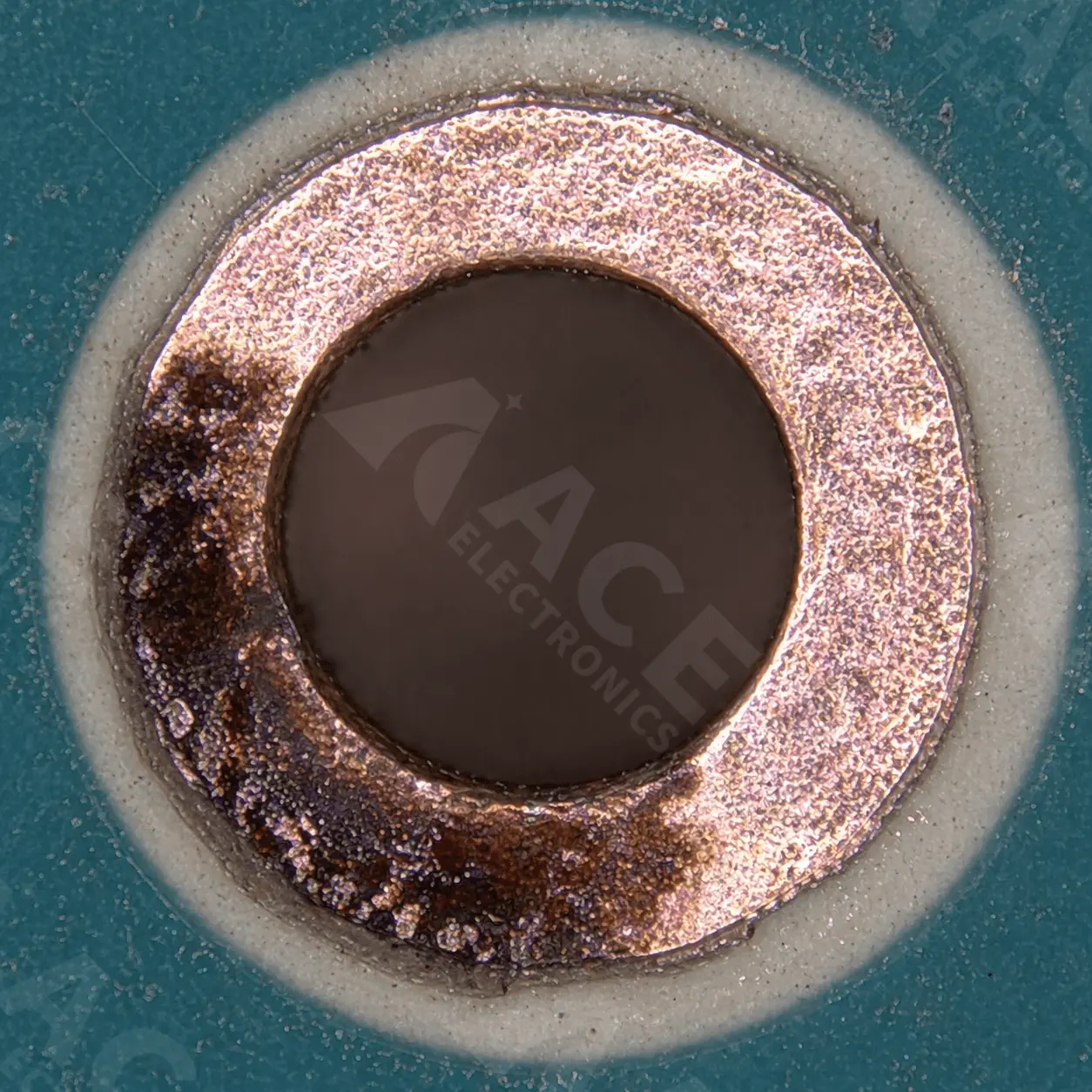
What Black Pad Failure Can Look Like
Black pad and phosphorus-rich layer problems may show up as:
- Poor wetting during soldering
- Weak solder joints
- Brittle fracture after shear or pull testing
- BGA opens after thermal cycling
- Intermittent electrical failures
- Cracked solder joints under vibration
- Dark or rough nickel surface after solder separation
- Abnormal SEM/EDS failure analysis results
For BGA, this is especially serious because the solder joints are hidden under the package. Visual inspection may not catch the defect. X-ray may detect some assembly defects, but black pad is often confirmed only through destructive analysis such as cross-section, dye-and-pry, SEM, EDS, pull testing, or shear testing.
In many failure analysis cases, black pad is confirmed only after the solder joint has already failed. Cross-section images may show an irregular or corroded nickel surface under the solder joint. SEM/EDS analysis may show nickel corrosion and phosphorus enrichment at the fracture interface.
This is why a board can pass normal visual inspection but still fail during pull testing, thermal cycling, or field use.
What Failure Analysis Usually Finds
When ENIG black pad is suspected, engineers usually do not rely on appearance alone. A board may pass normal visual inspection, but still show weak solder joints after reflow, pull testing, thermal cycling, or field use.
Failure analysis usually looks for several signs.
1. Nickel Corrosion Under the Gold Layer
The first thing to check is whether the electroless nickel layer has been seriously corroded during the immersion gold process.
In a normal ENIG cross-section, the nickel surface should be relatively continuous and uniform. If the immersion gold process attacks the nickel too aggressively, the cross-section may show deep corrosion spikes or uneven nickel attack below the gold layer.
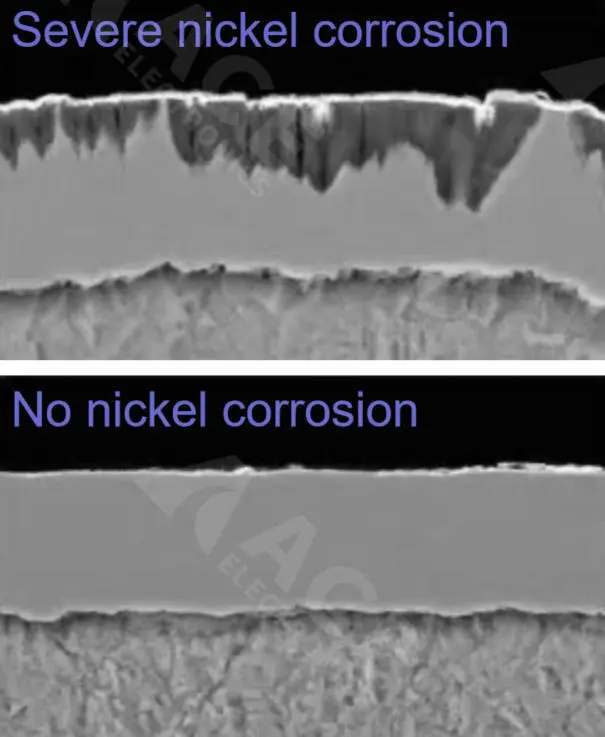
Cross-section analysis can show whether the nickel layer has been excessively corroded during the immersion gold process.
This matters because black pad is often linked to nickel corrosion. If the nickel layer has already been damaged before soldering, the solder joint may form on a weak interface.
2. Cracking or Mud-Crack Patterns on the Nickel Surface
After solder separation or surface analysis, engineers may inspect the nickel surface for dark cracks or mud-crack patterns.
If the nickel surface shows severe cracking, black or dark fractured areas, or local corrosion paths, it may indicate that the ENIG interface was weakened before or during soldering.
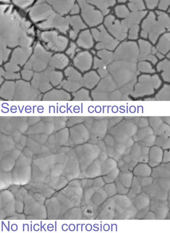
Severe cracking or mud-crack patterns on the nickel surface can be a warning sign of ENIG black pad risk.
This type of defect may not cover the whole pad. It can appear locally, especially in areas where plating chemistry, pad geometry, or surface condition made the nickel more vulnerable.
3. Excessive Gold Thickness
Gold thickness is another key point.
In ENIG, the immersion gold layer is very thin. It protects the nickel surface before soldering, but it is not meant to be a thick functional gold layer.
If the gold layer is too thick, the immersion gold reaction may have been too aggressive or too long. That increases the chance of nickel corrosion underneath.
For many ENIG specifications, designers should reference IPC-4552B or a customer-approved equivalent instead of only writing "gold finish" in the drawing. The supplier should control nickel and gold thickness by the agreed standard, often verified by XRF measurement.
4. Nickel Layer Too Thin or Poorly Controlled
The nickel layer has two important functions:
- It provides the main solderable surface.
- It works as a barrier between copper and the outer gold layer.
If the nickel layer is too thin, uneven, or poorly controlled, it may not provide a stable barrier. It can also become more vulnerable during the immersion gold process.
This is one reason PCB designers should not only specify ENIG by name. The fabrication notes should reference the required standard, and the PCB fabricator should be able to control nickel thickness and plating quality.
Before releasing files for PCB fabrication service, it is better to make the ENIG requirement clear in the fabrication notes.
5. Poor Solder Joint Strength
Black pad is often confirmed when the solder joint fails mechanically.
During pull testing, shear testing, or fracture analysis, a weak ENIG interface may separate at or near the nickel-phosphorus layer. The fracture may look brittle instead of ductile.
Typical findings may include:
- Low pull strength or shear strength
- Brittle separation at the ENIG interface
- Phosphorus enrichment near the fracture path
- Rough or corroded nickel surface
- Abnormal nickel-tin intermetallic formation
For BGA and fine-pitch packages, this is especially serious because the solder joints are hidden under the component. If your design uses BGA, also read our guide to the best PCB surface finish for BGA assembly.
6. Abnormal Gold Surface Appearance
Sometimes black pad risk is also associated with abnormal pad appearance before assembly.
Examples include:
- White or pale gold surface
- Dark or uneven pad color
- Local discoloration
- Unusual surface roughness
- Inconsistent appearance between pads
Visual appearance alone cannot confirm black pad. But if the gold surface looks abnormal and the gold thickness is also outside control limits, further inspection is needed.
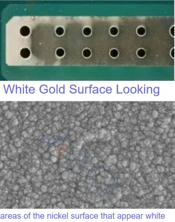
Abnormal gold surface color or local discoloration can be a warning sign, but black pad should be confirmed by proper inspection.
What Designers Should Learn From Failure Analysis
For PCB designers, the lesson is simple:
Black pad is not a layout mistake, but the design notes and supplier choice can decide whether the risk is controlled before fabrication.
A drawing that only says "gold finish" gives the supplier too much room. A better note should specify ENIG clearly, reference IPC-4552B or the customer-approved standard, and require controlled nickel/gold thickness where reliability matters.
For high-reliability boards, ENIG should be reviewed as part of the design release, not left as a late-stage purchasing choice.
Is ENIG Still a Good Surface Finish?
Yes. ENIG is still a strong surface finish when the process is controlled.
It is widely used because it provides:
- Flat pads for BGA and fine-pitch SMT
- Good solderability
- Better shelf life than OSP
- Lead-free compatibility
- Stable surface for high-density assembly
- Good performance for many industrial and high-reliability products
The correct conclusion is not "avoid ENIG."
The correct conclusion is:
Use ENIG when the design needs it, but specify it clearly and choose a qualified PCB fabricator.
For a broader comparison of common finishes, see our guide to PCB surface finish options.
When Designers Should Pay Extra Attention
You should review the ENIG requirement more carefully when the design has small solder joints or high reliability needs.
Pay extra attention when the PCB includes:
- BGA or micro-BGA
- 0.5 mm pitch or smaller components
- QFN or LGA packages
- HDI routing
- High layer count stackups
- Fine-pitch connectors
- High-current thermal pads
- Double-sided reflow
- Long storage before assembly
- Harsh operating environments
- Customer reliability testing
- Automotive, medical, aerospace, defense, or industrial use
In these cases, ENIG should be treated as part of the reliability design, not only as a purchasing option.
What PCB Designers Should Specify in Fabrication Notes
Before sending files for PCB fabrication service, do not leave the finish note vague.
Avoid unclear notes such as:
- Gold finish
- Gold plating
- ENIG finish
- Surface finish: gold
These notes may be too loose for high-reliability work.
A better fabrication note may include:
- Surface finish: ENIG
- Applicable standard: IPC-4552B or customer-approved equivalent
- Lead-free assembly compatible
- Nickel and immersion gold thickness per applicable specification
- PCB supplier to control ENIG process to prevent nickel corrosion / black pad risk
- Packaging and storage per supplier recommendation
For projects with stricter reliability requirements, add customer-specific requirements, inspection requirements, and acceptance criteria. For example:
- Surface finish: ENIG per IPC-4552B.
- Supplier shall confirm nickel/gold thickness by XRF.
- Cross-section or solderability test required if specified by customer quality plan.
- Boards must be packaged to protect solderability during storage and shipment.
The exact wording should match your customer requirement, industry requirement, and supplier capability.
Designer Checklist Before Releasing ENIG Boards
Before releasing a PCB with ENIG, review these questions:
- Does the board actually need ENIG?
- Are there BGA, QFN, LGA, CSP, or fine-pitch components?
- Is the surface finish note clear enough?
- Does the fabrication drawing reference IPC-4552B or a customer-approved ENIG standard?
- Are nickel and gold thickness requirements controlled by the chosen standard?
- Does the product have thermal cycling, vibration, drop, or long-life requirements?
- Is ENEPIG required for wire bonding or higher reliability margin?
- Will the boards be stored for a long time before assembly?
- Does the PCB fabricator have proven ENIG capability?
- Is any extra inspection required for the customer or application?
- Are solderability and packaging requirements clear?
- Has the assembly team reviewed the finish choice for BGA or fine-pitch risk?
This checklist is especially useful before prototype release, NPI build, or production transfer.
Should You Specify ENEPIG Instead?
Sometimes, yes.
ENEPIG adds a palladium layer between nickel and gold.
| Finish | Layer structure |
|---|---|
| ENIG | Copper / Nickel / Gold |
| ENEPIG | Copper / Nickel / Palladium / Gold |
The palladium layer helps separate nickel from the final immersion gold layer. This can reduce nickel corrosion risk and improve suitability for wire bonding or high-reliability applications.
ENEPIG may be worth reviewing when:
- The PCB requires wire bonding
- The product is high-reliability or mission-critical
- The design uses advanced packages
- The customer is concerned about ENIG black pad risk
- The cost of failure is much higher than the finish cost
- The end product is used in medical, aerospace, defense, automotive, or harsh industrial environments
ENEPIG is not necessary for every design. It costs more and may require more specialized supplier capability. For many BGA and fine-pitch SMT boards, ENIG is still the practical choice.
For a full comparison, read our guide to ENIG vs ENEPIG surface finish.
Does OSP Avoid Black Pad?
OSP does not have an electroless nickel layer or immersion gold layer, so it does not have ENIG black pad.
But OSP has different trade-offs.
OSP is more sensitive to:
- Storage time
- Handling
- Humidity
- Multiple reflow cycles
- Rework
- Uncertain assembly schedules
For cost-sensitive boards assembled soon after fabrication, OSP may work well. For BGA, fine-pitch, long storage, or high-reliability projects, ENIG may still be better.
For details, read our guide to OSP PCB surface finish.
What ACE Reviews Before PCB Fabrication
At ACE Electronics, we review ENIG as part of the PCB fabrication and assembly risk, not just as a surface finish name.
For ENIG boards, we may review:
- Gerber files
- Stackup
- Solder mask openings
- BGA pad design
- Fine-pitch component areas
- Surface finish notes
- Customer reliability requirements
- Storage and packaging expectations
- Assembly process requirements
- Whether ENIG or ENEPIG is more suitable
If the board is simple, ENIG may be unnecessary. If the board has BGA, fine-pitch, or high-reliability requirements, ENIG may be the right choice, but it should be specified and controlled correctly.
ACE provides PCB fabrication service for prototype, small-batch, and production boards, including ENIG surface finish review before manufacturing.
For projects that also need component sourcing, SMT assembly, testing, and shipment, ACE can support the full production flow as a turnkey PCBA factory.
Final Recommendation
ENIG black pad is a serious reliability issue, but it does not mean ENIG is a bad surface finish.
ENIG remains one of the most useful finishes for BGA, fine-pitch, and high-reliability PCB assembly. The real risk is poor ENIG process control or unclear fabrication requirements.
For PCB designers, the practical rule is:
- Use ENIG when the board needs flatness, shelf life, and stable solderability.
- Do not specify ENIG as a vague "gold finish."
- Reference a proper ENIG standard such as IPC-4552B when required.
- Ask whether ENEPIG is better for wire bonding or higher reliability margin.
- Choose a PCB fabricator with proven ENIG process control.
- Treat surface finish as part of design-for-manufacturing, not only as a quote item.
Before you release Gerber files, ask one question:
If a solder joint fails later, did my fabrication notes give the supplier enough information to control the ENIG risk?
If the answer is no, improve the notes before production.
Related Guides and Services
- For fabrication support, visit: PCB Fabrication Service
- For ENIG basics, read: What Is ENIG PCB Surface Finish?
- For ENIG upgrade decisions, read: ENIG vs ENEPIG Surface Finish
- For BGA projects, read: Best PCB Surface Finish for BGA Assembly
- For all common finish options, read: How to Choose PCB Surface Finish
- For cost-sensitive finish selection, read: What Is OSP PCB Surface Finish?
Frequently Asked Questions
What is ENIG black pad?
What is ENIG black pad?
ENIG black pad is a plating defect related to excessive corrosion of the electroless nickel layer during the immersion gold process. It can cause weak solder joints, brittle fracture, and reliability problems.
Is black pad normal for ENIG?
Is black pad normal for ENIG?
No. Black pad is not a normal ENIG condition. It is a process control problem. Properly plated ENIG should provide stable solderability and reliable assembly performance.
What is a phosphorus-rich layer in ENIG?
What is a phosphorus-rich layer in ENIG?
A phosphorus-rich layer is a phosphorus-enriched region at the solder joint interface. A thin layer can be part of the normal reaction, but an excessive or continuous phosphorus-rich layer can weaken the solder joint.
Can PCB designers prevent black pad?
Can PCB designers prevent black pad?
PCB designers cannot control the plating bath directly, but they can reduce risk by specifying ENIG clearly, referencing the correct standard, selecting a qualified PCB fabricator, and considering ENEPIG for higher-risk designs.
Should I specify IPC-4552B for ENIG?
Should I specify IPC-4552B for ENIG?
For many professional ENIG projects, IPC-4552B is commonly used as the ENIG specification. The exact requirement should match the customer standard, industry requirement, and PCB supplier capability.
Does ENEPIG eliminate black pad?
Does ENEPIG eliminate black pad?
ENEPIG can significantly reduce ENIG-related nickel corrosion risk because the palladium layer acts as a barrier between nickel and gold. However, ENEPIG still requires good process control and is not required for every board.
Is ENIG safe for BGA?
Is ENIG safe for BGA?
Yes. ENIG is widely used for BGA because it provides a flat and solderable surface. For high-reliability BGA projects, the key is to use clear specifications and a qualified PCB fabricator.
Should I choose OSP instead of ENIG to avoid black pad?
Should I choose OSP instead of ENIG to avoid black pad?
OSP does not have ENIG black pad because it does not use nickel or gold. But OSP has other risks, including shorter storage life and a narrower assembly window. The right choice depends on component package, storage time, reliability needs, and assembly process.
About the Author
Bill Ho is Sales Engineer and Chief Editor at ACE Electronics, with 10 years of experience in PCB fabrication and PCB assembly.
He writes practical technical content focused on manufacturability review, fabrication communication, and assembly risk reduction.