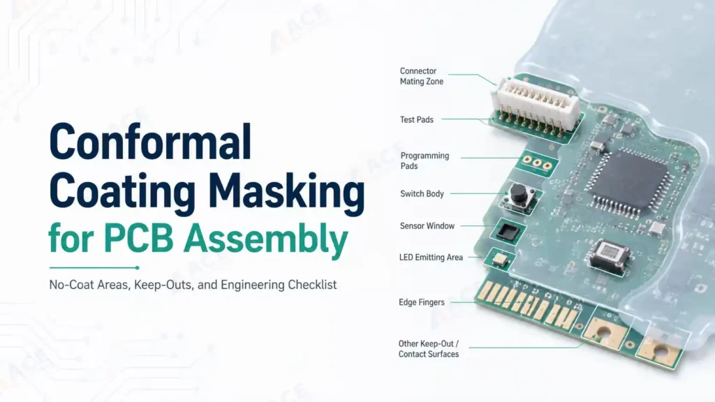
Conformal coating masking protects the PCB areas that must stay free of coating. Common no-coat areas include connectors, test points, programming pads, switches, sensors, LEDs, edge fingers, RF sections, grounding pads, thermal pads, and mechanical mating surfaces.
Clear masking requirements help your assembly partner quote accurately, plan the coating step, protect test access, and avoid rework. A marked drawing prevents more production questions than a written note.
Review this guide before RFQ, prototyping, or starting production.

The top side of a coated PCB assembly shows why connectors, test points, and exposed contact areas should be reviewed before masking.

The bottom side also needs a no-coat review because pads, contacts, vias, and assembly interfaces may appear on either side of the board.
What Is Conformal Coating Masking?
Conformal coating masking temporarily protects PCB areas that must stay uncoated. Protected areas typically require electrical contact, mechanical movement, optical clarity, RF performance, thermal transfer, test access, or final assembly contact.
Common terms include:
| Term | Meaning in a PCBA order |
|---|---|
| No-coat areas | Board areas or component surfaces that must stay free of coating |
| Keep-out areas | Zones where coating should be kept away because of function, access, or assembly fit |
| Coating-free zones | Marked board areas reserved for connectors, contacts, sensors, RF paths, test pads, or mechanical interfaces |
| Maskants | Materials used to protect those areas during coating, such as tape, dots, plugs, caps, boots, or peelable mask |
Masking is one step in the broader conformal coating process. Define the masking plan before coating begins. Late changes can disrupt quoting, fixtures, test sequence, inspection, and delivery.
Why No-Coat Areas Matter Before RFQ or Production
No-coat areas directly affect quotation and production planning. Each protected feature adds handling, setup, and inspection work. A board with one edge connector differs significantly from a board with multiple connectors, test pads, RF features, thermal contacts, and enclosure mating points.
| Engineering item to confirm | Why it needs masking | Production risk if unclear |
|---|---|---|
| Which connector surfaces must mate after coating | Coating can cover pins, sockets, shells, or insertion faces | Failed mating, failed functional test, extra cleaning |
| Which pads need testing or programming access later | Coated pads can block probes or programming access | Test delay, retest, coating removal |
| Which areas contact a housing, shield, ground, or thermal interface | Coating can insulate or interfere with contact | Grounding, heat transfer, or fit issues |
| Which LEDs, sensors, microphones, or optical windows must remain exposed | Coating can change light, sound, or sensing behavior | False readings or poor product function |
| Which RF areas require stable performance | Coating can change local dielectric conditions or contaminate contacts | RF tuning or signal problems |
Masking also affects lead time. Manual masking can take longer than coating itself when the board has many sensitive interfaces. For repeat production, fixtures or reusable masking boots often reduce labor when the same areas are protected every run.
Common No-Coat and Keep-Out Areas on PCB Assemblies
The exact no-coat areas depend on the product. The table below gives a practical starting point for a PCB assembly coating review.
| Area | Why it may need to stay uncoated | What to confirm |
|---|---|---|
| Connectors and sockets | Mating surfaces and pins need clean electrical contact | Which side, shell, pin field, or insertion face must remain clean |
| Test points | ICT, FCT, or probe access may be required | Whether testing happens before coating only or after coating too |
| Programming pads | Firmware loading or late updates may need pad access | Whether programming pads need post-coating access |
| Switches and buttons | Moving parts can bind if coating enters the mechanism | Which actuator, opening, or nearby pad needs protection |
| Sensors, microphones, and optical windows | Coating can block or change the sensing path | Which surface must remain exposed |
| LEDs, light pipes, and displays | Coating can affect clarity, brightness, or color | Whether the optical face or full component needs masking |
| Edge fingers and card contacts | Contacts must stay conductive and dimensionally clean | Top side, bottom side, bevel area, and mating length |
| RF antennas and RF contact areas | Coating can affect tuning or contaminate RF contacts | RF keep-out boundary and accepted coverage nearby |
| Grounding pads and shield contacts | Coating can create unwanted insulation | Contact surface and enclosure/shield requirement |
| Thermal pads and heat-transfer surfaces | Coating can interfere with thermal interface material | Thermal interface boundary and final heat path |
| Mechanical mating areas | Coating thickness can affect fit | Screw bosses, brackets, frames, clips, or enclosure contact points |
| Vias, slots, and open holes | Coating can wick through openings or reach the other side | Whether the feature should be masked, filled, tented, or left open |
Provide both top-side and bottom-side views. Marking only one side risks missing connectors, pads, contacts, vias, or enclosure interfaces on the other side.
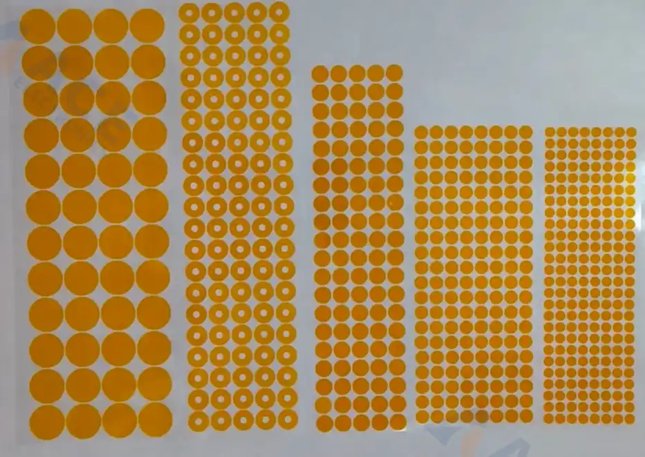
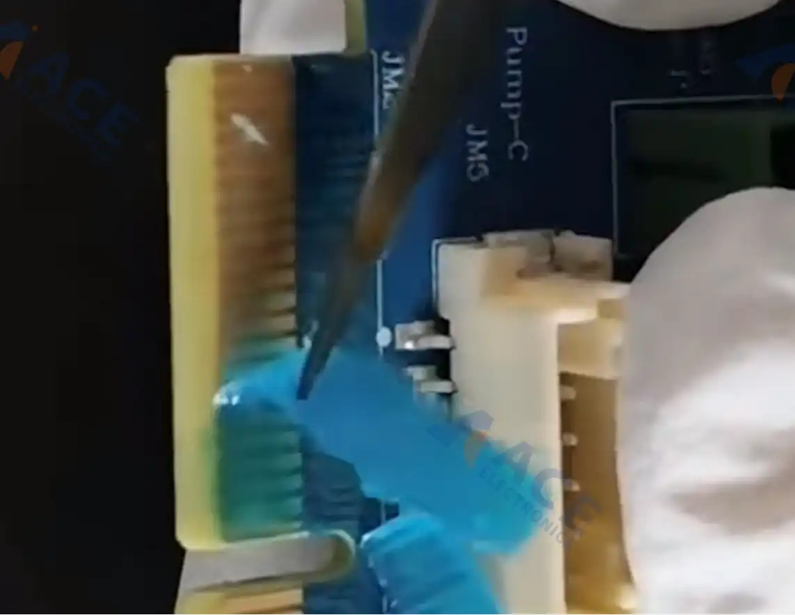
Masking dots or discs can protect small pads, vias, holes, and repeatable no-coat points across a PCB assembly.
Masking Methods Used in PCB Conformal Coating
Masking method selection depends on board geometry, access conditions, order quantity, and inspection requirements. Choose the method that fits the board layout and production scope.
| Method | Typical use | Buyer note |
|---|---|---|
| Tape | Straight edges, flat areas, edge fingers, larger zones | Labor depends on board access and edge shape |
| Dots or discs | Small round pads, vias, holes, repeatable small features | Useful when many small no-coat points repeat across boards |
| Plugs | Holes, sockets, ports, selected openings | Fit and removal access matter |
| Caps | Pins, posts, terminals, exposed shapes | Useful when the geometry allows a clean seal |
| Boots | Connectors or repeated complex shapes | More useful in repeat production or high masking labor orders |
| Peelable mask or liquid maskant | Irregular shapes, cavities, small complex areas | Removal and compatibility should be confirmed |
| Fixtures | Repeat production with repeatable placement | Setup adds planning time and may reduce repeated labor |
| Selective coating path | Automated coating around defined keep-outs | Clear no-coat definitions are still required |

Polyimide tape protects flat areas, straight edges, edge contacts, and larger no-coat zones before conformal coating.
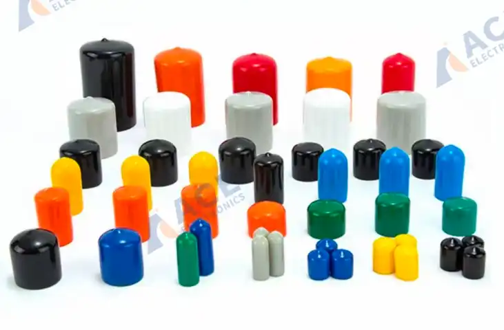
Vinyl caps protect pins, posts, terminals, and exposed component features when the geometry allows a clean temporary cover.
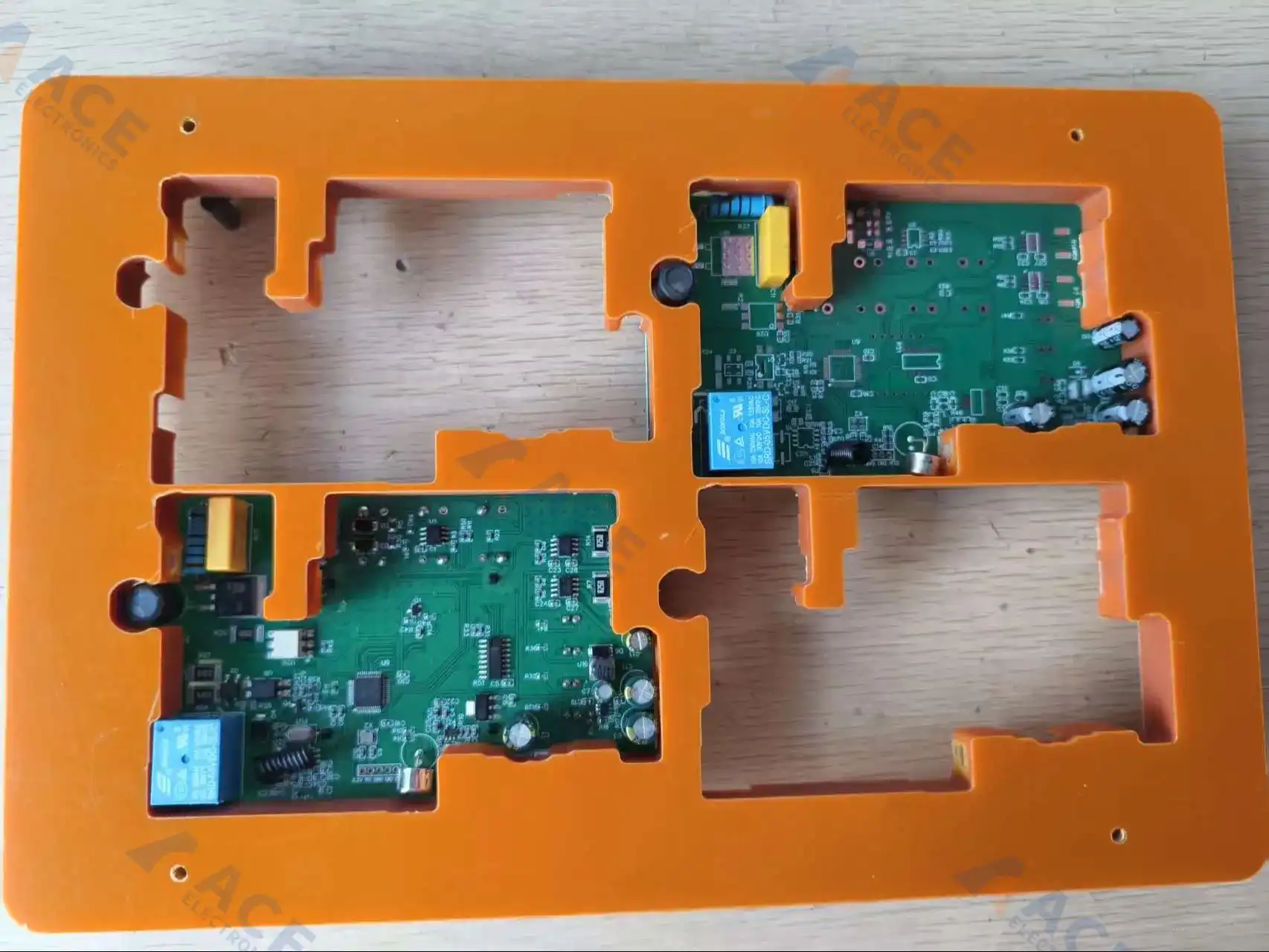
A customized coating fixture helps control repeatable placement, handling, and masking access during pilot or production runs.
What to Send Your Assembly Partner Before Quotation
A clear quote package helps the assembly partner estimate masking labor, plan test sequence, and confirm whether the coating scope fits the board layout.
Send these items before quotation:
- PCB Gerber files and assembly drawings.
- Top and bottom views with all no-coat areas marked.
- Board images with callouts when drawings are hard to interpret.
- BOM notes for sensitive parts, sensors, switches, LEDs, microphones, displays, connectors, and RF components.
- Test point and programming pad requirements.
- Test sequence before and after coating.
- Coating material if your team already specified one.
- Coating method if your product already requires a specific method.
- Grounding, shielding, thermal, and mechanical contact areas.
- Enclosure assembly or final product assembly requirements.
- Quantity, prototype plan, pilot run plan, and expected production run volume.
- Inspection criteria, coating standard, or customer acceptance requirement when applicable.
Use the checklist below during engineering review:
| Checklist item | Confirmed |
|---|---|
| Every top-side no-coat area is marked | |
| Every bottom-side no-coat area is marked | |
| Connectors identify the exact mating faces or pin fields | |
| Test points and programming pads are labeled | |
| Sensors, LEDs, displays, microphones, and optical windows are marked | |
| RF areas and antenna-related keep-outs are identified | |
| Grounding pads, shield contacts, and chassis contact areas are marked | |
| Thermal interface areas are identified | |
| Mechanical mating areas and enclosure interfaces are shown | |
| Post-coating testing, programming, or calibration needs are clear | |
| Final product assembly requirements are included | |
| Prototype, pilot run, and production quantities are stated |
This checklist helps your assembly partner judge whether masking will be straightforward, labor-intensive, fixture-dependent, or sensitive to later testing steps.
Peelable mask can protect irregular shapes, cavities, small complex areas, and local keep-outs where tape or caps are harder to apply.
Planning Masking in Your PCBA Production Order
When conformal coating is part of a PCBA order, the production review should cover assembly, firmware loading, functional testing, masking, coating, inspection, and final product assembly together. This prevents masking conflicts with later test access or enclosure fit.
Share your no-coat drawing before quotation. The review can then confirm whether connectors, test points, programming pads, sensors, RF areas, grounding pads, thermal interfaces, and mechanical mating areas need protection.
If testing happens before coating, confirm the test sequence early so masking does not block probe access later. For detailed test planning, see the PCBA programming and testing requirements. If the coated board goes into an enclosure, coordinate masking with the final product assembly plan.
For coating material and process decisions, start with the PCB conformal coating guide. For production support and quotation, see our PCB conformal coating services.
Frequently Asked Questions
What PCB areas should stay free of conformal coating?
What PCB areas should stay free of conformal coating?
Common areas include connectors, sockets, test points, programming pads, switches, LEDs, sensors, microphones, displays, edge fingers, RF antennas, grounding pads, shield contacts, thermal pads, and enclosure mating areas.
Do connectors need masking before conformal coating?
Do connectors need masking before conformal coating?
Most connectors need masking on the mating surface, pins, socket opening, or contact area. Mark the exact surfaces on the drawing. Some connector bodies can tolerate coating nearby.
Should test points and programming pads be coated?
Should test points and programming pads be coated?
Test points and programming pads should stay accessible when they are needed after coating. If all testing and firmware loading happen before coating, confirm whether post-coating access is still required for inspection, repair, or later updates.
Can LEDs, sensors, or optical parts be applied with conformal coating?
Can LEDs, sensors, or optical parts be applied with conformal coating?
Many LEDs, sensors, microphones, displays, and optical windows need clean exposed surfaces. Coating can affect light output, sensing accuracy, acoustic performance, or optical clarity.
Does selective coating remove the need for masking?
Does selective coating remove the need for masking?
Selective coating can reduce masking work when the machine path is well defined. Connectors, tight keep-outs, tall parts, vias, edge contacts, and sensitive interfaces may still need local protection.
What should I send to an assembly partner before quoting conformal coating?
What should I send to an assembly partner before quoting conformal coating?
Send Gerber files, assembly drawings, top and bottom no-coat markings, sensitive component notes, test and programming requirements, coating requirements, inspection criteria, production quantity, and final assembly requirements.