Not long ago, a customer asked us for a 12-layer PCB quote — 1oz copper, plus pricing for 2oz and 5oz. Our engineer reviewed the Gerber files and found the outer layer spacing was only 6 mil, and the inner layers were 4 mil. That meant the design could not run 5oz at all.
What Is PCB Copper Thickness and Why It Matters for Your Quote
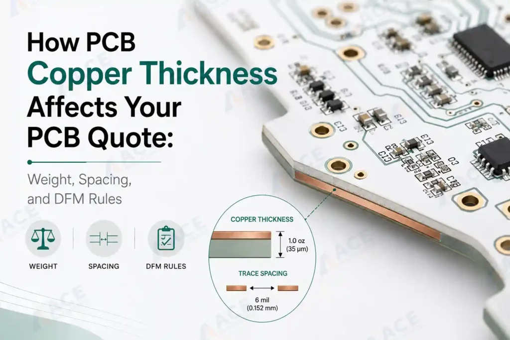
Copper thickness in a PCB is the height of the copper foil layer after lamination and plating. In the PCB industry, this thickness is expressed in ounces (oz) — but what is being measured is weight per square foot, not thickness directly.
If you take 1 ounce of copper and flatten it evenly across 1 square foot of surface area, the resulting foil will be approximately 1.37 mils thick (about 0.0348 mm, or 34.8 µm). That is the standard reference for what the industry calls "1oz copper."
Copper Weight vs. Thickness — the Standard Conversion Table
| Copper Weight (oz/ft²) | Thickness in mils |
Thickness in mm |
Thickness in µm |
|---|---|---|---|
| 0.5 oz | 0.69 mil |
0.017 mm |
17.5 µm |
| 1 oz | 1.37 mil |
0.035 mm |
34.8 µm |
| 2 oz | 2.74 mil |
0.070 mm |
69.6 µm |
| 3 oz | 4.11 mil |
0.104 mm |
104.4 µm |
| 4 oz | 5.48 mil |
0.139 mm |
139.2 µm |
| 5 oz | 6.85 mil |
0.174 mm |
174.0 µm |
| 6 oz | 8.22 mil |
0.209 mm |
208.8 µm |
When you request a PCB quote and ask for 2oz copper instead of 1oz, you are asking the PCB manufacturer to double the copper thickness on those layers. That does not simply mean "use a thicker sheet of foil." It changes the etching process, the lamination parameters, the plating time, and in many cases the minimum trace spacing the factory can guarantee.
The thicker the copper, the more process steps and the tighter the tolerance control — and the higher the cost.
A Real 12-Layer PCB Quote Story: What Happened When the Customer Asked for 2oz and 5oz
Here is what happened with this 12-layer PCB order — and why copper thickness is a pricing factor.
The customer's original RFQ was straightforward:
"12-layer PCB, FR4, 1oz copper on all layers, standard lead time."
But then the customer came back with:
"Can you also quote 2oz and 5oz copper? I want to see the price difference."
That is when our engineering team opened the Gerber files and started the DFM review.
A customer asked for a 12-layer PCB quote with 1oz copper and also wanted pricing for 2oz and 5oz copper.
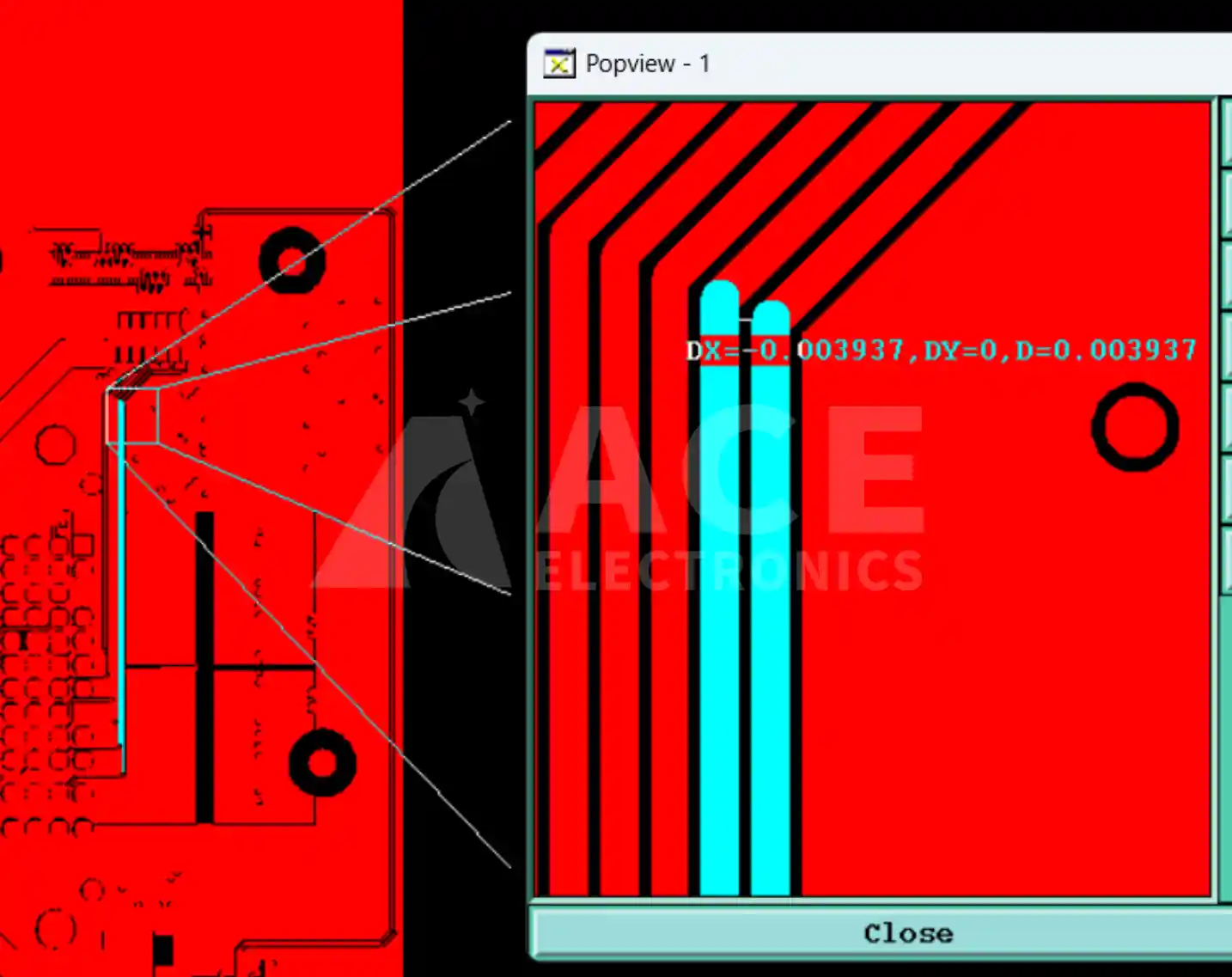
Outer Layer with 6 mil Spacing — Why 2oz Was the Ceiling
The outer layers of this design had trace-to-trace and trace-to-pad spacing as tight as 6 mil in several areas. When you increase copper thickness, the etching process becomes more aggressive because the chemical etchant must remove more material vertically — and while it does that, it also etches sideways (undercut). With thicker starting foil:
- Etch undercut increases.
- The minimum reliable trace spacing grows wider.
- Fine-pitch features become impractical to guarantee.
For 2oz copper on outer layers, most fabricators need a minimum spacing of around 6 to 8 mil. This design was right at that boundary — 2oz was possible, but 5oz was not. To put the gap in perspective: even 3oz (4.11 mil thick foil) already requires minimum spacing around 10 mil. For 5oz (6.85 mil), the required spacing is even wider — far beyond what this 6 mil design allowed.
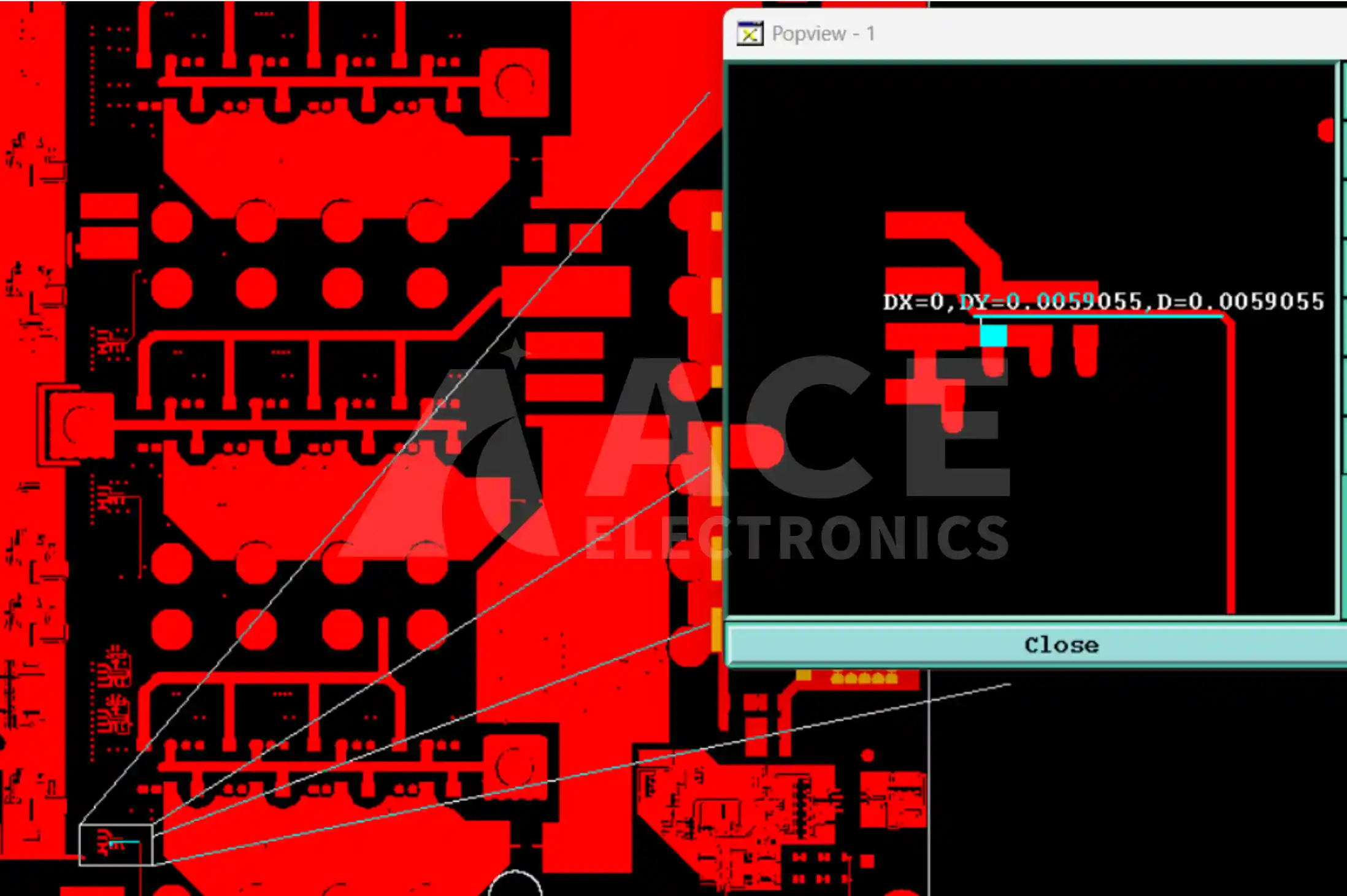
Gerber review: outer layer spacing was 6 mil, inner layers were 4 mil. These numbers set the hard limits on achievable copper thickness.
Inner Layer with 4 mil Spacing — Why 1oz Was the Hard Limit
The inner layers were even tighter — spacing down to 4 mil. On inner layers, the copper foil is sandwiched between dielectric layers during lamination, which creates different manufacturing conditions than outer layers. The same etching physics apply, but with an additional constraint: inner layers typically start with thinner copper and do not receive the same plating buildup as outer layers during through-hole plating.
For 1oz copper on inner layers, most fabricators specify a minimum spacing of roughly 3.5 to 4 mil. This design was already at the edge. Increasing to 2oz inner-layer copper would require spacing closer to 6-8 mil — well beyond what this design allowed.
The hard engineering answer was clear: outer layers capped at 2oz, inner layers capped at 1oz.
The second PCB model had 4 mil spacing on both inner and outer layers, limiting every layer to 1oz copper — 2oz and 5oz were not manufacturable.
How Copper Thickness Directly Affects PCB Manufacturing Cost
Let us break down exactly where the cost comes from when you request thicker copper.
Why Thicker Copper Makes PCB Fabrication More Difficult
Going from 1oz to 2oz (or higher) is not just a material swap.
- Etching time increases. Thicker copper needs longer immersion in the etchant bath. Longer etching means more lateral etching (undercut), which forces wider trace spacing and limits the minimum trace width the factory can guarantee.
- Plating time increases. For outer layers, the copper foil is further built up during the copper plating step. Thicker starting foil means more plating current and time to achieve proper hole-wall plating in vias.
- Lamination pressure and heat profiles change. A stackup with mixed copper weights — some layers at 1oz, others at 3oz or 5oz — requires careful lamination parameter adjustment to avoid uneven resin flow, voids, or delamination.
- Yield drops. The tighter the process window, the more boards are rejected during inspection. Lower yield per panel means higher unit cost for the boards that pass.
All of this adds up: a 2oz PCB typically costs 20% to 50% more than the same design in 1oz, and 5oz can be 70% to 150% more. The exact number depends on layer count, board size, and how close your spacing is to the process limits.
Raw Copper Material Cost
Beyond the manufacturing difficulty, there is a simpler reason thicker copper costs more: you are buying more copper. A 2oz board uses literally twice the copper weight of a 1oz board on every layer that carries the heavier foil. The copper foil itself is a commodity — its price tracks the global copper market, and fabricators pass that cost through to your quote.
As of May 2026, LME copper is trading near $13,200 per metric ton, up roughly 45% from the $9,100/ton level seen in early 2025. When the raw material price moves up, the cost difference between 1oz and 2oz gets wider — because every ounce of extra copper on your board is now more expensive to procure before it even reaches the factory floor.
This is also why selective heavy copper makes a real difference in your quote.
Inner Layer Heavy Copper vs. Outer Layer Heavy Copper — Different Cost Drivers
Inner-layer heavy copper costs differently than outer-layer heavy copper. The reason is the manufacturing flow:
- Outer layers start from a copper-clad laminate with a given foil weight, then receive additional copper plating during the through-hole plating step. Achieving a specific finished outer copper thickness means controlling both the starting foil weight and the plating deposition. The challenge is that thick outer copper makes etching and surface finish (ENIG, HASL) harder to control, which can push yield down.
- Inner layers are etched and laminated, and they do not receive the same plating buildup as outer layers. To get 3oz or 5oz on an inner layer, the fabricator must start with heavy copper-clad laminate from the material supplier — which is more expensive and has longer lead times. However, the inner-layer process skips the electroplating and surface-finish steps that complicate outer-layer thick copper.
There is also a hidden cost that is easy to miss: board area and layer count. When copper thickness forces you to widen traces and spacing (for example, moving from 1oz at 4mil spacing to 2oz at 6mil or 8mil), the same routing density no longer fits. If the board size is fixed, you may need more layers to route the same design. Adding layers or increasing board size often costs more than the copper material itself.
Selective Heavy Copper: Only Thicken the Layers That Carry High Current
After our pcb engineer told me this client's 12-layer board could not run 5oz everywhere, I asked the client a practical follow-up:
"Which layers actually need to carry high current? We can put thicker copper only on those specific layers, and keep the rest at standard weight."
The answer came back: the power distribution layers — inner layers 4 and 6 — were the only ones carrying significant current. The other inner layers handled signal routing and low-current logic.
This is called selective heavy copper, and it is one of the most effective ways to control cost on a multilayer PCB. Instead of ordering 5oz copper on all 12 layers (which was physically impossible anyway), the customer could:
- Keep outer layers at 2oz, which aligns with a 6 mil trace/space DFM rule at most fabricators
- Put 3oz or 5oz heavy copper only on several power layers
- Keep the remaining signal layers at 1oz
The result: the board still handles the required current, but the fabrication cost is far lower than an all-heavy-copper stackup — and the design stays within manufacturable limits.
However, there is one hard rule that comes with selective heavy copper: copper symmetry.
DFM Rules: Copper Weight vs. Minimum Trace Spacing
Before you request a quote with heavy copper, check your trace spacing against the copper weight you want. Here is a practical reference table based on what most fabrication partners can reliably achieve.
Spacing Limits by Copper Weight — Reference Table
| Copper Weight | Minimum Trace Width | Minimum Trace Spacing | Typical Applications |
|---|---|---|---|
| 0.5 oz (inner) | 3 mil |
3 mil |
High-density digital, fine-pitch BGA |
| 1 oz | 3.5 mil |
3.5 mil |
Standard digital, low-power analog |
| 2 oz | 6 mil |
6–8 mil |
Power supplies, motor drivers |
| 3 oz | 8 mil |
8–10 mil |
High-current power, automotive |
| 4 oz | 10 mil |
12–14 mil |
Heavy power distribution |
| 5 oz | 12 mil |
14–16 mil |
Bus bars, extreme current |
Note: These values are typical guidelines. Your fabrication partner's exact limits depend on their equipment, chemistry, and process control. Always confirm during DFM review.
What Happens When Your Design Exceeds the Spacing Limit
If you request 5oz copper on a design with 4 mil spacing, here is what actually happens — the etching step cannot fully clear the narrow gaps between traces, which results in copper bridges (shorts) or unpredictable trace widths. The factory will either reject the design outright or ask you to respin the layout with wider spacing.
This is the single most common back-and-forth delay in heavy-copper PCB quoting. The customer asks for thick copper because they need high current capability, but the design was laid out with standard 1oz spacing rules — assuming the traces can be packed tightly. When the DFM review catches the mismatch, the quote stalls.
The simplest way to avoid this: before you finalize a design intended for heavy copper, check your spacing against the table above. If your design has 4 mil or 5 mil spacing anywhere, 1oz copper on those layers is likely your ceiling — regardless of what you would prefer to order.
Copper Symmetry
When our customer asked whether only inner layers 4 and 6 could be made thick copper, our engineer confirmed it was possible — with one condition:
"Yes, but the stackup has to be symmetric. For example, on a 6-layer board, L1 and L6 should have the same copper weight. L2 and L5 should match. L3 and L4 should match. Do not design asymmetric copper — the material becomes very expensive and the board will warp."
When a multilayer PCB goes through the high-temperature lamination press and then cools down, the copper layers and the dielectric material expand and contract at different rates. If the copper distribution is unbalanced — heavy copper on one side of the stackup center, light copper on the other — the board experiences uneven internal stress. The result is:
- Board warping and twisting after lamination, making assembly difficult or impossible.
- Delamination risk at the interface between heavy and light copper layers.
- Higher material cost, because the fabricator must source special prepregs and adjust the lamination cycle to compensate — and even then, the yield is lower.
Symmetry Rules for 4-Layer, 6-Layer, and Multilayer PCBs
| Layer Count | Symmetry Rule |
|---|---|
| 4-layer | L1 copper weight = L4 copper weight. L2 = L3. The board center is between L2 and L3. |
| 6-layer | L1 = L6. L2 = L5. L3 = L4. Each pair mirrors across the board center. |
| 8-layer | L1 = L8. L2 = L7. L3 = L6. L4 = L5. |
| 10-layer / 12-layer | Same principle: copper weight must mirror across the center plane of the stackup. |
In the customer's 12-layer case, the power layers (L4 and L6) that needed heavy copper were not mirror pairs. L4's mirror is L9, and L6's mirror is L7. To maintain symmetry, if L4 got thick copper, L9 also had to get thick copper — even if L9 only carried low-current signals. This is the hidden cost of selective heavy copper: you often have to add thick copper to layers that do not need it, just to keep the stackup balanced.
How to Specify Copper Thickness When Requesting a PCB Quote
The most common mistake buyers make when requesting a PCB quote with heavy copper is leaving the copper thickness unspecified. If your Gerber files do not include a stackup table — and standard Gerber RS-274X does not encode copper thickness — the fabricator will default to 1oz on all layers. When the boards arrive with thinner copper than you expected, it is almost always because the thickness was never communicated.
Here is a practical checklist for your next quote request.
A Practical Checklist for Your RFQ
- [ ] Specify finished copper thickness per layer. Not "1oz" — specify whether you mean starting foil weight or finished copper thickness after plating. Outer layers gain additional plating during through-hole processing, so a 1oz starting foil can become approximately 1.5oz to 2oz finished copper on outer layers. Be explicit: "Finished outer layer copper: 2oz. Finished inner layer copper: 1oz."
- [ ] Include a stackup table. Your fabrication drawing or a separate stackup document should list each layer number, its function (signal, ground, power), and its finished copper weight.
- [ ] Check your trace spacing against your copper weight request. If your design has 4 mil spacing on inner layers and you are asking for 2oz inner copper, flag this before sending the RFQ — or expect the quote to come back with a note asking you to respin.
- [ ] If using selective heavy copper, mark which layers carry high current. Do not make the fabricator guess. A simple note — "L4 and L9 carry 30A peaks; all other layers are signal" — lets the factory propose the most cost-effective stackup.
- [ ] Confirm the symmetry rule with your design. If you need heavy copper on one inner layer, its mirror pair across the stackup center must match. Budget for that extra layer in your cost estimate.
- [ ] Ask for a DFM review before ordering. A proper fabrication partner will run your Gerber files through a DFM check and flag spacing-vs-copper-thickness mismatches before you commit to a production order. If your supplier does not offer this, find one that does.
Frequently Asked Questions
What is the standard PCB copper thickness?
What is the standard PCB copper thickness?
The industry default is 1oz copper (1.37 mils / 34.8 µm finished thickness on inner layers). Most fabricators assume 1oz on all layers unless you specify otherwise in your stackup table or fabrication notes.
How does copper thickness affect PCB cost?
How does copper thickness affect PCB cost?
Thicker copper increases cost because it requires longer etching time, tighter lamination control, additional plating, and often wider minimum trace spacing — all of which reduce panel yield. A 2oz design can cost 20–50% more than the same design in 1oz, and 5oz or higher can be 50–100% more expensive, depending on layer count and spacing constraints.
What is the minimum trace spacing for 2oz copper? For 5oz?
What is the minimum trace spacing for 2oz copper? For 5oz?
For 2oz copper, most fabrication partners require a minimum trace spacing of 6–8 mil. For 5oz copper, the minimum spacing typically increases to 8–10 mil on outer layers and may be even wider on inner layers. These numbers vary by factory — always confirm with your supplier's DFM guidelines.
Can I use different copper thicknesses on different layers of the same board?
Can I use different copper thicknesses on different layers of the same board?
Yes. This is called selective heavy copper. You can put thicker copper only on the layers that carry high current. However, the stackup must remain symmetric — each layer's mirror pair across the board center must have the same copper weight. Asymmetric "yin-yang copper" causes board warping and increases cost.
Why does my PCB supplier say my design cannot use 5oz copper?
Why does my PCB supplier say my design cannot use 5oz copper?
The most common reason is that your trace spacing is too tight. Copper etching becomes less precise as foil thickness increases. If your design has 4 mil or 6 mil spacing, those gaps may not etch cleanly with 5oz copper, leading to shorts, inconsistent trace widths, or outright manufacturing failure. The DFM review catches this before production.
What is copper symmetry, and why does it matter for multilayer PCBs?
What is copper symmetry, and why does it matter for multilayer PCBs?
Copper symmetry means the stackup has matching copper weights on mirror layers across the board center (e.g., L1 = L6, L2 = L5, L3 = L4 on a 6-layer board). Without symmetry, uneven thermal expansion during lamination causes board warping, twisting, and delamination — all of which make the board unusable for assembly.
Do I need to specify copper thickness in my Gerber files?
Do I need to specify copper thickness in my Gerber files?
Standard Gerber RS-274X files do not encode copper thickness. You must specify finished copper thickness per layer in your fabrication drawing, stackup table, or a separate readme document. If you do not specify it, the fabricator will default to 1oz on all layers.
What information should I include about copper thickness when requesting a quote?
What information should I include about copper thickness when requesting a quote?
Include a stackup table listing each layer's finished copper weight, your target trace spacing, and a note about any layers that carry high current. If your design has tight spacing (below 6 mil), flag this early so the fabricator can confirm what copper weights are achievable before quoting.
If you are preparing a multilayer PCB order that involves heavy copper or mixed copper weights, share your Gerber files and stackup requirements with our engineering team. We run a free DFM review on every quote request and will tell you honestly which copper thicknesses your design can support — before you commit to an order.
Get a PCB fabrication quote with DFM review →
If your design is ready for assembly after PCB fabrication, ACE also supports full turnkey PCBA including component sourcing, SMT and through-hole assembly, conformal coating, and functional testing. For projects involving heavy copper designs like battery management systems, see our BMS case study for an example of 5oz copper with Parylene coating.