PCB Fabrication Service
From Rapid Prototype to Mass Production.
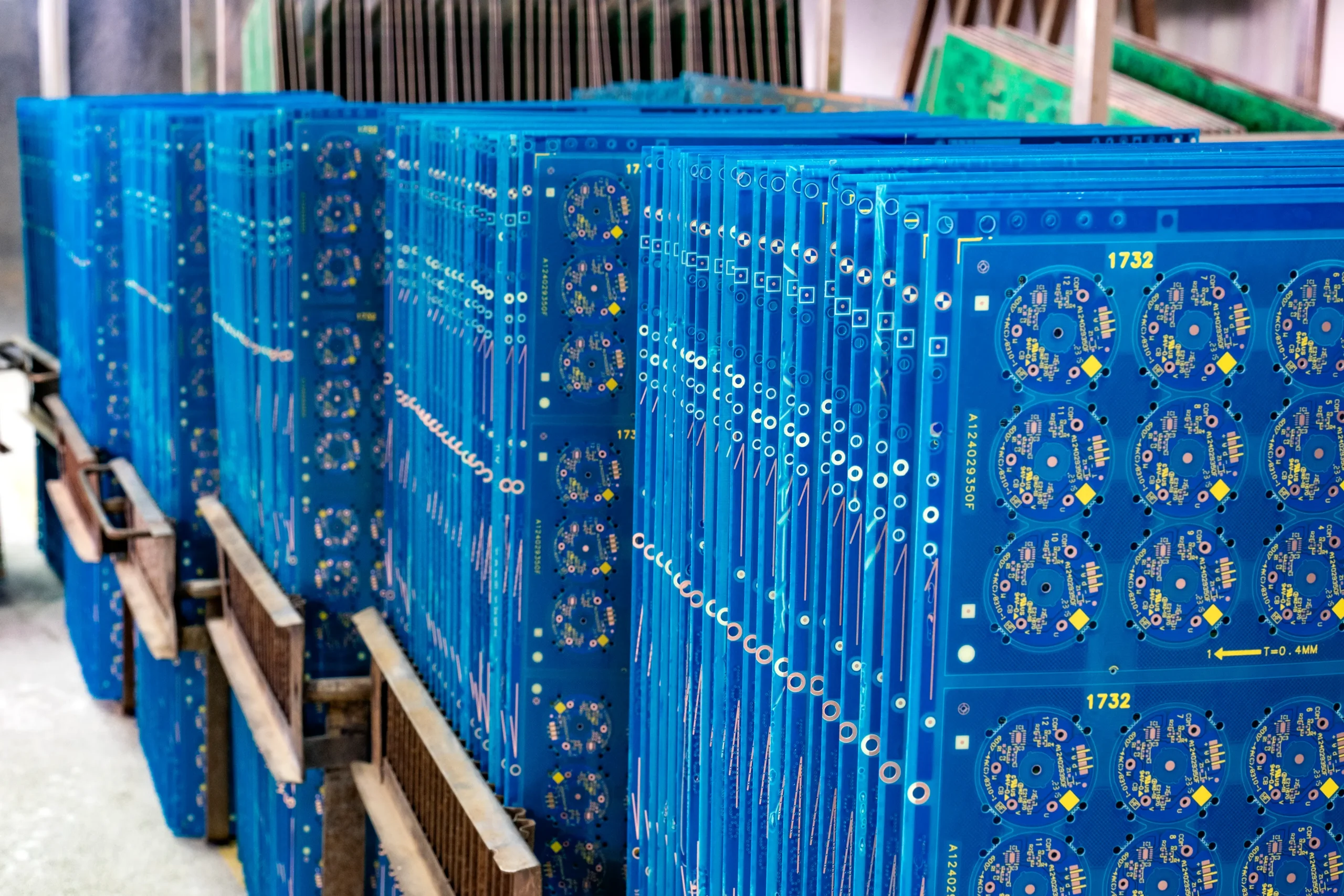
Our PCB Manufacturing Capabilities
Precision Printed circuit board fabrication capabilities for prototypes, engineering validation, and production runs.
IATF 16949 & UL Certified.

PCB Fabrication Capabilities at ACE Electronics
Common bare PCB requirements supported across prototype orders, engineering validation, and production runs. Exact limits depend on stackup, material, copper weight, line spacing, and final application.
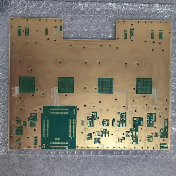
Materials
- FR4 and high Tg FR4
- Rogers, Isola, and PTFE-based materials
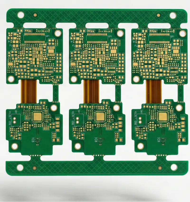
- Polyimide for flex circuits
- Aluminum and copper base materials
Key Processes
- Blind and buried vias
- Via filling and fine line fabrication
- Controlled impedance
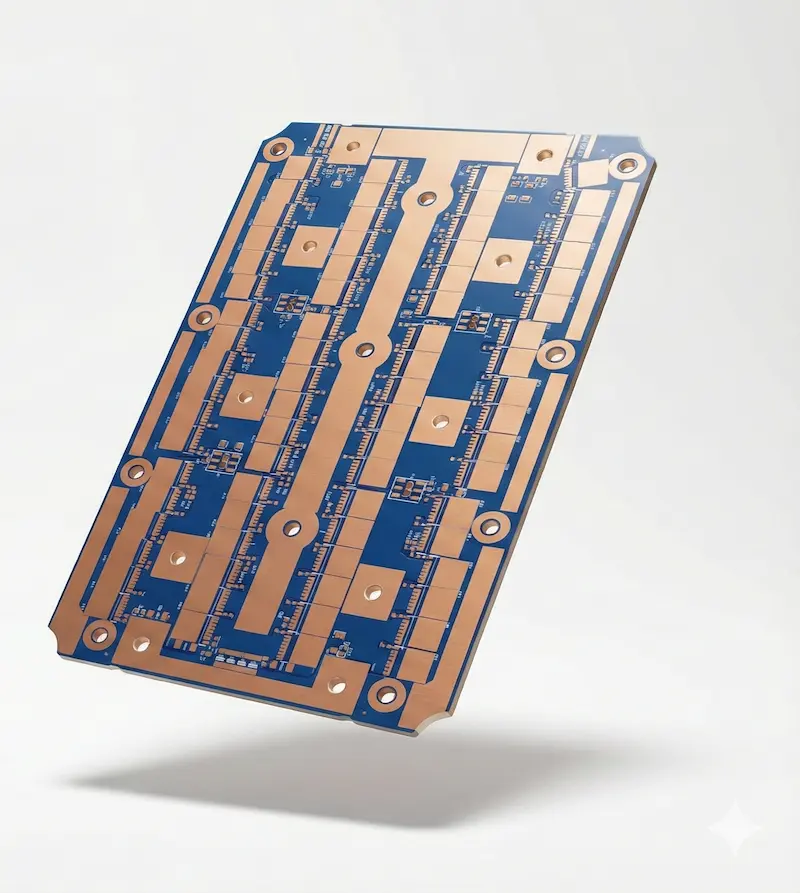
- Heavy copper, edge plating, and surface finishes
Quality Controls
- AOI inspection
- 100% electrical testing
- Micro-section when needed
- Impedance verification when required
Circuit Board Manufacturing Process
In printed circuit board fabrication, a bare PCB order moves through engineering review, material preparation, imaging, drilling, plating, surface finishing, testing, and final inspection before shipment or assembly.
Engineering Review
Gerber, drill files, stackup, copper weight, material, surface finish, and controlled impedance requirements are checked before production.
Material Preparation
FR4, high Tg FR4, Rogers, Isola, polyimide, aluminum, copper base, and other approved materials are prepared according to the stackup.
Imaging, Etching & Lamination
Circuit patterns are transferred to copper layers, etched, inspected, and laminated into the required multilayer structure.
Drilling & Via Formation
Mechanical drilling, laser drilling, blind and buried vias, and via filling are processed according to the board design.
Plating & Outer Layer Processing
Copper plating, pattern plating, outer layer imaging, and etching form the final conductive paths and plated through holes.
Solder Mask & Surface Finish
Solder mask, legend, ENIG, HASL lead-free, OSP, immersion silver, immersion tin, or hard gold are applied as required.
Testing & Final Inspection
AOI, electrical testing, dimensional checks, impedance verification, and micro-section review are used when required by the project.
Packing, Shipment or Assembly
Finished bare boards are packed for shipment or transferred to PCB assembly, firmware loading, testing, coating, or final product assembly.
Bare PCB Manufacturing Quality Checks
Verified Performance.
Every PCB is manufactured under strict process control with full inspection and traceability to ensure consistent electrical performance and long‑term reliability.
- IPC Class 2 / Class 3 Manufacturing
- 100% Electrical Testing
- AOI, X‑Ray & Micro‑Section Analysis
- IATF 16949 Certified Quality System
Material Integrity
We only source from authorized distributors (Shengyi, KB, Rogers). Zero tolerance for grey-market scraps or fake materials.
Process Control
100% AOI (Automated Optical Inspection) & E-Test included in every batch to ensure electrical continuity.
Certified By

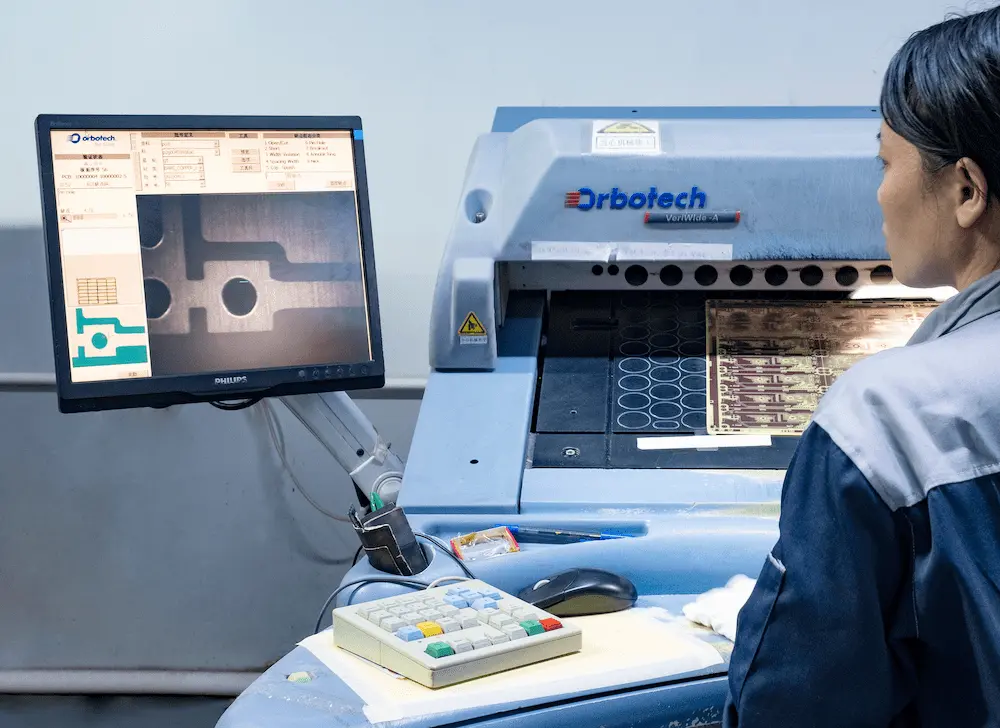
PCB Automated Optical Inspection
At ACE Electronics PCB Factory
How to Start a PCB Fabrication Order
From Gerber files and stackup requirements to finished bare boards or PCB assembly.
Upload Files
Gerber RS-274X & BOM
Free DFM Check
Within 12 Hours
PCB Fabrication
Quick Turn / Mass Prod
Electrical Test
100% E-Test / AOI
FQC & Packing
Final QC / Vacuum Pack
Ship or Assembly
Global Delivery / ACE Electronics SMT Lines
Frequently Asked Questions
Q
What files do you need for PCB fabrication?
What files do you need for PCB fabrication?
Please provide standard Gerber files (RS-274X) along with your NC drill files, or ODB++ formats. Include a read-me text file with stack-up details, material requirements, surface finish, and board thickness for a precise quote.
Q
What materials do you use for PCB manufacturing?
What materials do you use for PCB manufacturing?
We use a wide range of materials depending on your application. This includes standard FR4, High-TG FR4, Rogers, Isola, Polyimide for flex circuits, and Aluminum/Copper bases for high thermal conductivity needs.
Q
What surface finishes can you provide?
What surface finishes can you provide?
We offer multiple surface finishes including HASL (Lead-Free), ENIG (Electroless Nickel Immersion Gold), OSP, Immersion Silver, Immersion Tin, and Hard Gold plating for edge connectors (Gold Fingers).
Q
What are your fabrication capabilities for HDI boards?
What are your fabrication capabilities for HDI boards?
We support advanced HDI routing with any-layer interconnection, blind and buried vias, and plated via filling. Our minimum line width and spacing can reliably reach down to 2 mil (50 µm).
Q
Do you perform electrical testing on bare PCBs?
Do you perform electrical testing on bare PCBs?
Yes. Every manufactured board undergoes 100% electrical testing to ensure there are no open or short circuits before shipping. We use Flying Probe testing for prototypes and E-test fixtures for mass production.
Q
What is the typical lead time for bare PCB boards?
What is the typical lead time for bare PCB boards?
Standard PCB prototypes typically take 3 to 5 days. For advanced boards (HDI, Rigid-Flex, Multilayer) or mass production, the lead time ranges from 2 to 3 weeks depending on complexity and volume.
Need PCB Assembly or Final Product Assembly?
If your project needs more than bare PCB manufacturing, ACE can continue with PCB assembly, protective coating, testing, and final product assembly.
PCB Assembly
SMT and THT assembly with 01005 component capability. Complete with AOI, X-ray inspection, and IC programming.
Explore PCBA ServicesParylene Coating
In-house Parylene coating for assembled electronics that need moisture, chemical, and dielectric protection in demanding applications.
Learn About Parylene CoatingBox Build Assembly
Enclosure assembly, cable harnesses, PCB mounting, labeling, functional testing, and packing for final product assembly.
View Box Build ServiceNeed a complete manufacturing partner?
Explore Turnkey Assembly ServicesStart Your PCB Fabrication Project Today!
Send your Gerber files, stackup, material requirements, quantity, and target lead time for a PCB fabrication quote.
Quick Response via WhatsApp
Get instant answers to your questions
Connect directly with our technical team for immediate assistance.
We typically respond within 30 minutes during business hours.
Business Hours: Mon-Fri 9:00-18:00 (GMT+8)