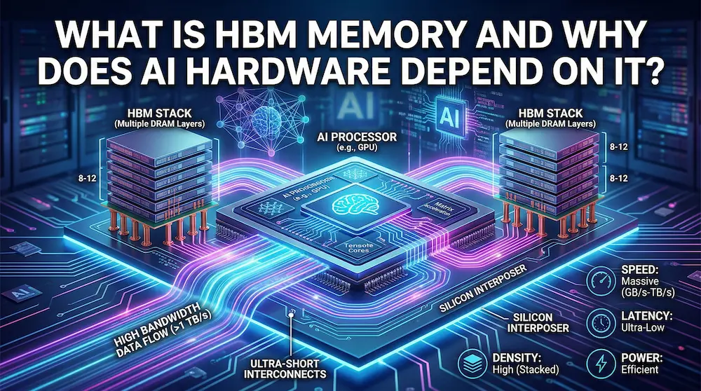
Having trouble keeping up with all the AI hardware terms like HBM, DRAM1, and NAND2? You're not alone. This powerful memory is critical for AI's future.
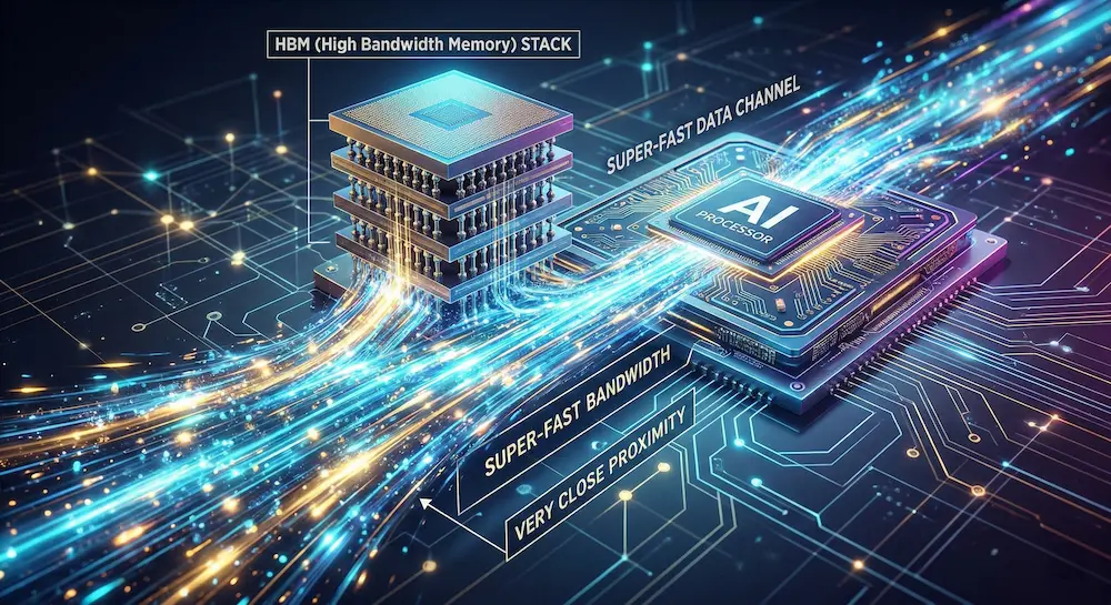
HBM, or High Bandwidth Memory3, is a special type of DRAM designed for extreme performance. It acts as a super-fast data channel for AI chips by stacking memory vertically and placing it extremely close to the processor, enabling the massive data flow required for AI tasks.
That's the quick answer. But to really understand why HBM is such a big deal for AI, we need to see how it compares to the memory chips you're more familiar with. The details are what make this technology a true game-changer, so let's keep going.
How is HBM Different from Regular Memory like DRAM and NAND?
The world of memory chips is full of confusing acronyms. You've heard of DRAM and NAND, but where does HBM fit in? Let's clear up the confusion.
HBM is a high-performance version of DRAM, built for speed. While standard DRAM is fast and NAND is for long-term storage (like an SSD), HBM uses a special 3D stacking4 design to achieve much higher data bandwidth5, making it ideal for data-hungry AI processors6.
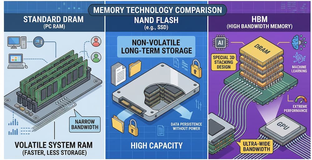
To understand HBM, we first need to know about the two most common memory types. DRAM1 (Dynamic Random-Access Memory) is very fast but loses its data when the power is off. It's perfect for tasks your computer is actively working on. NAND flash is what's in your SSD; it's slower but keeps your data safe even without power. More informaiton you could click to check my another blog article.
HBM is a member of the DRAM1 family, but it's a performance monster. It's a special type of DRAM1 redesigned purely for speed, specifically to feed data to powerful processors without delay. Think of it not as a replacement for all memory, but as a specialized component for high-performance computing7.
Here’s a simple breakdown:
| Memory Type | Main Feature | Volatility | Best For... |
|---|---|---|---|
| DRAM | Speed | Volatile | Active tasks, system RAM |
| NAND | Storage Persistence8 | Non-Volatile9 | Long-term storage, SSDs, USB drives |
| HBM | Bandwidth (Speed) | Volatile10 | High-performance computing, AI processors |
What Makes HBM so Fast for AI Chips?
Everyone says HBM is incredibly fast, but what's the secret sauce? The technical jargon can be intimidating, but the core ideas are actually quite easy to understand.
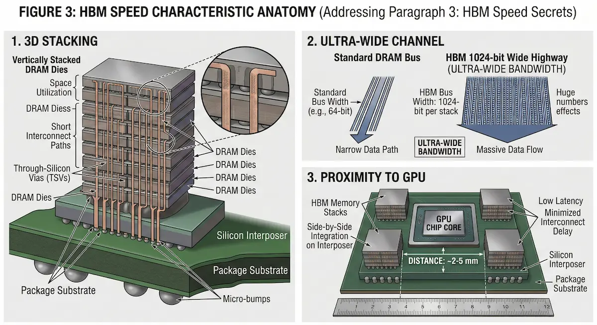
HBM's speed comes from three key features: 3D stacking, which packs more memory into a smaller space; an ultra-wide data channel for parallel data transfer; and its extremely close proximity to the GPU11, which drastically reduces data travel time and latency12.
Imagine an AI chip is a top chef cooking a complex meal. The data are the ingredients. With traditional memory, the ingredients are stored in a distant warehouse. The chef constantly has to wait for a small cart to bring them over. This waiting is what slows things down. HBM solves this with three clever tricks.
1. 3D Stacking
Instead of spreading memory chips out on a board, HBM stacks them vertically like a layer cake. This saves a ton of space and shortens the data paths.
2. Ultra-Wide Data Channel
HBM has a super-wide, 1024-bit highway for data. It's like having hundreds of lanes instead of just a few, allowing a massive amount of data to move all at once.
3. Ultra-Close Connection
HBM is placed right next to the chef (the GPU). It's like having a huge, multi-level spice rack right by the stove. The chef can grab any ingredient instantly. This combination means the AI chip never has to wait for data and can work continuously at full speed.
What Does an HBM Chip Actually Look Like on the Inside?
We've used analogies like layer cakes and highways, but what does an HBM package physically look like? The internal complexity of these chips can seem like magic.
An HBM package places the GPU or CPU in the center, surrounded by stacks of HBM. These components are mounted on a silicon 'interposer' which connects them. This entire assembly then connects to a substrate and finally to the main circuit board (PCB) via BGA13
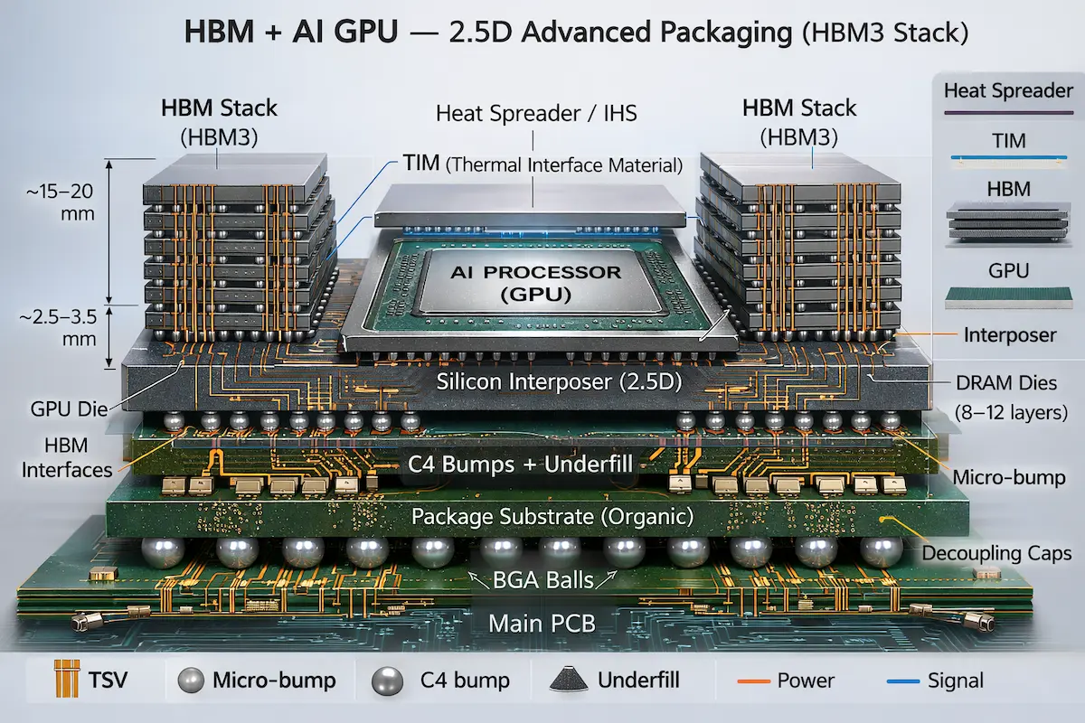
If we could peel back the layers of an AI accelerator, we'd see a masterpiece of engineering. The GPU11 or CPU die sits in the middle. It is surrounded by several HBM stacks. Each stack is a vertical tower of DRAM1 chips connected by tiny tunnels called Through-Silicon Vias14 (TSVs). But how does it all connect to the main board? It's a multi-step process.
- Micro Bumps: The GPU and HBM stacks are connected to a silicon base layer called an 'interposer' using thousands of tiny solder points called micro bumps.
- Interposer: This interposer acts as a high-speed communication bridge between the GPU and all the HBM stacks.
- BGA13 Balls: The interposer is then mounted on a package substrate, which finally connects to the main printed circuit board (PCB) using a grid of larger solder balls (BGA13).
The final chip, despite being only the size of your palm, contains an incredibly dense and complex network of connections, which is why manufacturing it is so challenging.
What Does the Future Hold for HBM Technology?
The tech world never stops moving. HBM is amazing now, but what comes next? As AI demands grow, memory technology must evolve even faster to keep up.
The future of HBM is focused on even higher bandwidth and more layers. HBM3 already offers huge gains, and the upcoming HBM4 standard aims to break the 1TB/s bandwidth15 barrier. This continuous innovation creates a significant technological challenge for any new competitors entering the market.
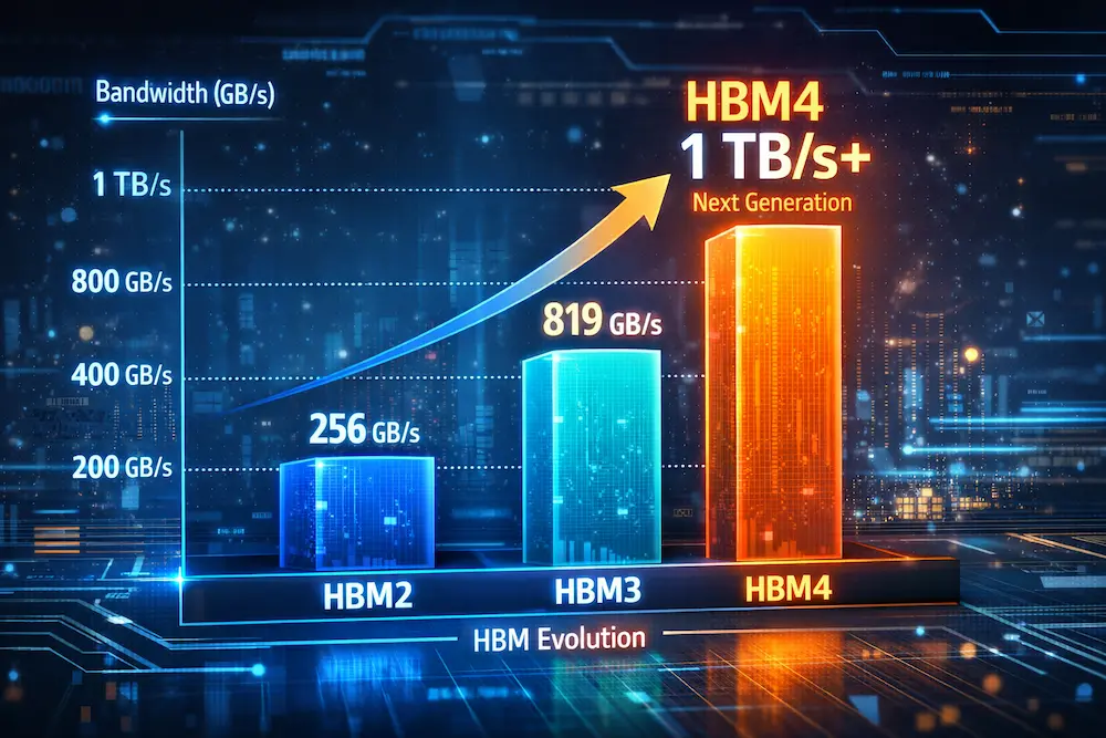
The relentless pace of AI development is pushing memory technology to its limits. The current generation, HBM3, is already impressive, with bandwidths reaching around 819 GB/s per stack. It also allows for more layers to be stacked vertically, all while managing power consumption better than its predecessors. But the industry isn't stopping there. The next generation, HBM4, is already in development. Experts predict it will push bandwidth even further, potentially breaking the 1 Terabyte-per-second (1TB/s) barrier. It will likely feature even more stacked layers. This constant push for more performance creates a huge technological moat. For any company trying to catch up, the investment in research, development, and advanced manufacturing required to compete at this level is enormous. It ensures that only a few key players can produce this critical AI component.
Conclusion
In short, HBM is the high-speed data backbone for modern AI. Its unique 3D design is essential for feeding powerful processors, making it a critical component for future innovation.
Need Help with purchasing HBM?
At ACE Electronics, we have 15 years of experience in electronic components and PCBA services. We have helped many clients choose the right memory for their projects—from factory devices to car electronics. Whether you need help picking memory types or finding hard-to-get chips, our team can guide you through the choices and supply issues. If you need memory chips or full PCBA support, visit our Components Sourcing page. We look forward to helping you build great products.

+++FAQ+++
- What exactly is HBM?
HBM (High Bandwidth Memory) is a specialized, high-performance variant of DRAM designed specifically for AI and high-performance computing. Unlike standard DRAM chips that lie flat on the motherboard, HBM uses 3D vertical stacking and sits directly adjacent to the processor to eliminate data bottlenecks and deliver massive bandwidth.
- How does HBM differ from DRAM and NAND?
While standard DRAM provides fast, volatile memory for general computing and NAND offers slower, non-volatile storage for SSDs, HBM is a purpose-built DRAM optimized exclusively for bandwidth. It serves as a high-speed data pipeline directly feeding powerful processors like GPUs, rather than acting as general system memory or long-term storage.
- What makes HBM so fast?
HBM achieves its speed through three key innovations: vertical 3D stacking that shortens signal paths, an ultra-wide 1024-bit data bus that transfers massive amounts of data in parallel, and its physical placement directly beside the GPU, which drastically reduces data travel time (latency).
- What does an HBM chip look like internally?
An HBM package places the GPU at the center, surrounded by several vertical stacks of memory dies. These components connect via a silicon interposer—a high-speed bridge—and link to the main circuit board through BGA solder balls, with Through-Silicon Vias (TSVs) creating vertical pathways through the stacked layers.
- Where is HBM actually used?
HBM is primarily found in AI accelerators, data center GPUs, and supercomputers where massive data throughput is critical. It is not used in consumer devices like laptops because it is prohibitively expensive and must be permanently soldered close to the processor during manufacturing.
- What is the future of HBM technology?
The industry is currently transitioning from HBM3 (offering ~819 GB/s per stack) to HBM4, which aims to exceed 1TB/s bandwidth with even more stacked layers. This rapid evolution creates a high barrier to entry, ensuring that only advanced manufacturers like SK Hynix, Samsung, and Micron can produce this critical AI infrastructure.
+++FAQ+++
Learn about DRAM's role in computing and its comparison with HBM for better understanding. ↩
Discover the applications of NAND flash memory and how it complements other memory types. ↩
Explore the importance of HBM in AI technology and how it enhances performance. ↩
Understand the benefits of 3D stacking in memory technology and its impact on speed. ↩
Find out how data bandwidth affects AI performance and the role of HBM in this context. ↩
Discover the characteristics of AI processors and their dependence on advanced memory. ↩
Explore the field of high-performance computing and its reliance on advanced memory solutions. ↩
Explore this resource to understand how storage persistence impacts data retention and performance in modern computing. ↩
Explore this resource to understand the key differences between non-volatile and volatile memory, crucial for grasping memory technology. ↩
Understanding volatility in memory types like DRAM and HBM is crucial for grasping their performance and application in AI. ↩
Explore the significance of GPUs in AI and how they interact with memory technologies. ↩
Learn about latency and its impact on computing efficiency, especially in AI applications. ↩
Explore this resource to understand BGA's role in connecting HBM chips, enhancing performance in AI hardware. ↩
Discover how TSVs enhance the performance of HBM and contribute to its efficiency. ↩
Learn about the implications of achieving 1TB/s bandwidth in memory technology. ↩