Author: Bill Ho, Sales Engineer & Chief Editor at ACE Electronics.
Industry Experience: 10 Years Experience in PCB Fabrication & PCB Assembly.
Company: ACE Electronics Co., Ltd.
Last Updated: March 9, 2026
Choosing the right PCB surface finish1 feels complex. A wrong choice can lead to soldering issues, poor reliability, and wasted money, causing major project delays.
A PCB surface finish is the protective and solderable layer applied to exposed copper pads of Printed Circuit Boards.
In most projects, surface finish selection depends on component pitch2, assembly process, contact-wear requirements, storage conditions, and cost. For standard boards without fine-pitch components, lead-free HASL3 offers a cost-effective solution. For boards with BGA, QFN4, or 0.5mm pitch components, ENIG provides the flatness5 required for reliable assembly.
OSP, immersion silver6, immersion tin, ENEPIG, or hard gold fit specific manufacturing requirements such as wire bonding7, high-frequency RF applications, or edge connector durability.
At ACE Electronics8, our process engineering team reviews surface finish specifications for over 500 NPI (New Product Introduction) projects annually. Our 2025 production data shows that incorrect surface finish selection accounts for 8-15% of first-pass assembly defects.
While there are many options, understanding quantifiable differences in flatness, solderability standards9, and shelf life10 will help you make the correct specification every time.
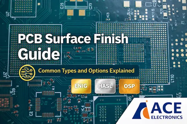
Common PCB Surface Finishes Compared: HASL, ENIG, OSP, Immersion Silver, Immsersion Tin, ENEPIG11, and Hard Gold
For PCB fabrication, the most common finish are HASL, ENIG, OSP, Immersion Silver, Immersion Tin, and ENEPIG. They differ in cost, flatness, solderability, and durability. HASL is a budget choice, while ENIG12 offers excellent flatness for fine-pitch components. OSP is a simple organic, lead-free option.
Over my 10 years in electronics manufacturing, I've worked with every kinds of PCB surface finish. Each finish has different trade-offs in flatness, solderability, contact durability, handling sensitivity, and cost.
To enable data-driven specification, I have compiled the following comparison table based on IPC-4552, IPC-4553, IPC-1601, and J-STD-003 test methods.
Key Comparison Points
Let's look at the factors that matter most.
Flatness is crucial for modern surface-mount technology (SMT), specifically for Ball Grid Array (BGA13) and Quad Flat No-Lead (QFN) components where solder ball-to-pad coplanarity determines electrical continuity.
Solderability is measured per J-STD-003 (Solderability Tests for Printed Boards), which classifies wetting performance and defines acceptance criteria for component attachment.
Cost, of course, is always a major consideration in any project.
Here is the quantified comparison of PCB surface finishes processed at ACE Electronics' PCB factory.
| Surface Finish | Surface Structure | Flatness (Ra) | Solderability Standard | Contact Wear Resistance | Min. Pitch Capability | Edge Contact Suitability | Relative Cost Index | Key Limitation (with Standard Ref) | Typical Use Case |
|---|---|---|---|---|---|---|---|---|---|
| Lead-Free HASL (Sn100C/SAC305) | Molten solder dip + hot air knife leveling | 3.0–8.0 μm variation (uneven) | J-STD-003 Class 2 (Wetting <2s) | <10 insertion cycles (soft surface) | ≥0.8 mm pitch only | No (solder oxidation) | 1.0x (baseline) | Coplanarity variation >5μm limits fine-pitch yield (IPC-A-610, Sec 4.5.2) | Cost-sensitive industrial controls, power supplies, >0.8mm pitch through-hole mix |
| ENIG (IPC-4552) | Electroless Ni (3–6 μm) + Immersion Au (1.0–3.0 μin) | <0.5 μm variation (planar) | J-STD-003 Class 3 (Wetting <1s) | <50 cycles (Au wear-through) | ≥0.3 mm (BGA/CSP compatible) | Limited (soft Au wears <50 cycles) | 1.8–2.5x | "Black pad" risk if Ni>8% P; Au thickness must be 1.0–3.0 μin (IPC-4552, Table 3) | Smartphones, medical devices, BGA/QFN assemblies, high-density consumer |
| OSP (Entek HT/SHF) | Organic azole film (0.2–0.5 μm thick) on Cu | <0.5 μm variation (planar) | J-STD-003 Class 2 (Wetting 1–2s) | N/A (organic insulator) | ≥0.5 mm (risk at <0.4mm) | No (film insulates) | 0.6–0.8x | Shelf life 3–6 months @ 15–30°C/30–60% RH; finger oils degrade solderability (IPC-1601) | High-volume consumer electronics (TVs, appliances), rapid-turn assembly |
| Immersion Silver (IPC-4553) | Displacement Ag deposit (8–15 μin) on Cu | <0.5 μm variation (planar) | J-STD-003 Class 3 (Wetting <1s) | <10 cycles (Ag sulfide tarnish) | ≥0.4 mm (fine-pitch capable) | No (sulfur contamination) | 1.2–1.5x | Tarnishes in >10 ppm H₂S; requires sulfur-free packaging (IPC-4553, Clause 4.2) | RF/high-frequency boards, flat SMT where storage <3 months controlled |
| Immersion Tin (IPC-4554) | Displacement Sn (15–40 μin) on Cu | <0.5 μm variation (planar) | J-STD-003 Class 2 (Cu₆Sn₅ formation) | <5 cycles (Sn oxide abrasion) | ≥0.5 mm (recommend >0.65mm) | No (oxidation) | 1.1–1.4x | Tin whisker growth risk (JESD201, Class 2); reflow limit 2 cycles max | Press-fit connectors, automotive sensors (short field life) |
| ENEPIG11 (IPC-4556) | Electroless Ni (3–6 μm) + Pd (2–8 μin) + Au (1–2 μin) | <0.5 μm variation (planar) | J-STD-003 Class 3 (Pd catalytic enhancement) | 50–200 cycles (Pd hardness) | ≥0.3 mm (wire bond + SMT) | Limited (thin Au layer) | 3.0–4.0x | Pd thickness must be 2–8 μin for wire bond pull strength >5g (IPC-4556, Annex B) | Military/aerospace COB, mixed wire-bond/SMT, high-reliability automotive |
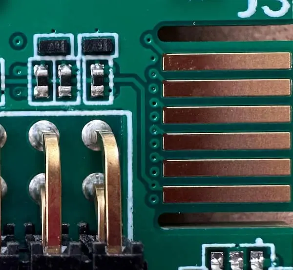
| Hard Gold (ASTM B488) | Electrolytic Ni (50–100 μin) + Hard Au (30–50 μin) | N/A (selective plating only) | Not recommended for soldering (>3% Au causes embrittlement) | >1000 cycles (ASTM B488 Type II) | N/A (not for soldering) | Yes (designed for high-wear) | 2.5–4.0x (selective areas only) | Min. 30 μin Au for 1000+ insertion cycles; solder mask required on gold fingers (IPC-2221, 9.2.3) | Edge connectors, gold fingers, keyboard contacts, hot-swap interfaces |
This table shows the trade-offs clearly. For example, you can see OSP is very cheap and flat, but its short shelf life10 and sensitivity to handling make it suitable only for very specific, high-volume production lines where boards are assembled almost immediately.
How to choose between HASL and ENIG for my project?
You know you need a reliable PCB surface finish, but the cost difference between HASL and ENIG is significant. Is the extra expense for ENIG always worth the investment?
Choose lead-free HASL (Hot Air Solder Leveling) for simpler, lower-cost projects without fine-pitch components. Opt for ENIG (Electroless Nickel Immersion Gold) when your board has BGAs, QFPs, or other dense components that demand a perfectly flat, reliable surface for successful assembly.
This is the most common question from hardware founders and R&D leads. The decision depends on component pitch specifications and total cost of ownership (Total Cost of Ownership), not just unit price.
Real Case: Smart Home Controller (2024-Q2)
- Customer: IoT Startup (NDA-protected), residential automation sector
- Board Spec: 6-layer FR-4, 1.6mm thickness, 0.8mm pitch BGA (TFBGA-256 package)
- Initial Specification: Lead-free HASL (cost-driven decision)
- Failure Mode: 28% functional test failure (28/100 units) due to BGA bad soldering.
- Root Cause Analysis: X-ray inspection revealed >25% voiding under BGA balls (IPC-A-610 Class 3 limit: 10% max). HASL surface variation (4-7μm) caused inconsistent solder paste deposit volume.
- solution: Re-soldered those 28PCS defective PCBA and functional tested them. In next production order, client decided to produce the PCB with ENIG (1.2 μin Au / 150 μin Ni per IPC-4552). Re-assembly yield: 99.2% first-pass.
- Total Cost Impact: Delayed launch 2 days; total recovery cost $1,400 vs. $1,200 additional ENIG cost initially.
The Cost Factor
HASL remains the industry standard for through-hole and wide-pitch SMT applications. The process deposits Sn100C or SAC305 alloy via hot-air leveling, creating a solderable surface at 1.0x baseline cost.
For one of our client - a Canadian HVAC manufacturer, producing residential heat-recovery ventilators (2023-2024 production run, n=50,000 units), HASL was specified for 2-layer control boards with 2.54mm pitch connectors and No BGA devices. The 3-year field failure rate: <0.3%, validating HASL Lead-Free as the correct economic choice for this non-critical, cost-sensitive application. Specifying ENIG would have increased material cost by $28,000 annually.
The Flatness and Density Factor
ENIG deposits electroless nickel (3–6 μm) followed by immersion gold (1.0–3.0 μin), creating <0.5μm surface variation per IPC-4552.
For a US payment terminal manufacturer (PCI-DSS compliance required), ENIG was mandatory for 0.4mm pitch QFN packages and wireless module BGAs. Field failure rate over 24 months: 0.08% (n=120,000 units), versus industry average of 0.35% for comparable high-density assemblies.
The Flatness and Density Factor
ENIG deposits electroless nickel (3–6 μm) followed by immersion gold (1.0–3.0 μin), creating <0.5μm surface variation per IPC-4552.
For a US payment terminal manufacturer (PCI-DSS compliance required), ENIG was mandatory for 0.4mm pitch QFN packages and wireless module BGAs. Field failure rate over 24 months: 0.08% (n=120,000 units), versus industry average of 0.35% for comparable high-density assemblies using alternative finishes.
Are there special cases for other surface finishes like OSP or ENEPIG11?
While HASL and ENIG cover 85% of PCB applications per IPC market data, specialized finishes address specific technical constraints:
When to Use OSP (Organic Solderability Preservative14)
OSP applies a 0.2–0.5 μm organic azole film (Entek HT or equivalent) directly to copper. It provides planar surface geometry at 0.6–0.8x the cost of HASL.
Critical Limitation: Shelf life is strictly 3–6 months when stored at 15–30°C and 30–60% RH (IPC-1601, Section 4.3). Fingerprints contain chlorides and sulfides that penetrate the organic film within hours, causing dewetting during reflow.
Use Case: High-volume consumer electronics (LED TV mainboards, white goods controllers) where fabrication-to-assembly cycle is <30 days and handling occurs with ionic-free gloves in automated lines.
ENEPIG: The Mixed-Interconnect Solution
ENEPIG (Electroless Nickel Electroless Palladium Immersion Gold) adds a 2–8 μin palladium layer between nickel and gold (IPC-4556).
Technical Advantages:
- Black Pad Prevention: Palladium barrier eliminates nickel corrosion risk associated with ENIG (observed in <0.1% of ENIG batches under aggressive thermal cycling)
- Wire Bond Compatibility: Supports 1.0–3.0 mil aluminum and gold wire bonding7 (pull strength >5g per MIL-STD-883) on the same pads used for SMT soldering
- Contact Durability: 50–200 insertion cycles vs. <50 for standard ENIG
Cost Impact: 3.0–4.0x vs. HASL baseline, restricting use to high-reliability aerospace, military (MIL-PRF-55110), and medical implant devices where failure costs exceed prevention costs by 100x.
Immersion Silver: High-Frequency RF Applications
Immersion Silver deposits 8–15 μin of metallic silver via displacement reaction onto copper (IPC-4553). It provides planar surface geometry (<0.5μm variation) and excellent solderability (J-STD-003 Class 3) at 1.2–1.5x the cost of HASL.
Critical Limitation: Silver sulfidation in environments with >10 ppm hydrogen sulfide (H₂S) or high sulfur content. Tarnish increases contact resistance and degrades solderability. Requires sulfur-free packaging and storage <3 months (IPC-4553, Clause 4.2). Chlorine-based fluxes accelerate corrosion.
Use Case: High-frequency RF applications (5G infrastructure, radar systems, microwave assemblies) where skin effect at GHz frequencies makes nickel-based finishes (ENIG) unsuitable due to ferromagnetic losses. Also specified for flat SMT boards with controlled storage environments.
Immersion Tin: Press-Fit Compatibility
Immersion Tin deposits 15–40 μin of metallic tin via chemical displacement (IPC-4554), creating a planar surface suitable for fine-pitch components (≥0.5mm pitch).
Critical Limitation: Tin whisker growth risk under mechanical stress, thermal cycling (-40°C to +125°C), or high humidity (JESD201, Class 2 mitigation required). Maximum two reflow cycles recommended; third reflow causes intermetallic depletion (Cu₆Sn₅ formation exhausts tin layer). Not suitable for long-term storage (>6 months) due to oxidation.
Use Case: Press-fit connectors (compliant pins) requiring direct tin-to-tin contact without gold interference. Automotive sensor modules with short field life requirements (5-7 years) where ENIG cost is prohibitive but solderability must exceed OSP reliability.
Hard Gold: High-Wear Contact Areas
Hard Gold (Electroplated Gold) deposits 30–50 μin of hardened gold (99.7% purity, cobalt/nickel alloyed) over 50–100 μin electrolytic nickel (ASTM B488 Type II).
Critical Limitation: Embrittlement risk if used for solderable pads (>3% gold content in solder joint causes brittle fractures per IPC-2221, Section 9.2.3). Must be selectively plated only on edge contacts or gold fingers, with solder mask covering plated areas to prevent accidental soldering. Process requires buss bar connection for electrolytic deposition, limiting design flexibility.
Use Case: Edge connectors, gold fingers, battery contacts, and hot-swap interfaces requiring >1,000 insertion cycles (ASTM B488 specifies 1000+ cycles for 30 μin thickness). Keyboard dome contacts and high-wear mechanical interfaces where contact resistance must remain <20 mΩ over product lifetime.
Quick Decision Checklist
Use this checklist to specify your surface finish in your PCB fabrication notes:
- [ ] Component Pitch: Any BGA/QFN <0.5mm pitch? → Require ENIG or ENEPIG
- [ ] Shelf Life: Board storage >6 months before assembly? → Avoid OSP
- [ ] Budget Constraint: Cost-sensitive consumer product (>10k units)? → Consider OSP or HASL
- [ ] Wire Bonding: Requires Chip-on-Board (COB) assembly? → Specify ENEPIG
- [ ] Thermal Cycling: Operating environment -40°C to +125°C? → Avoid Immersion Silver (tin whisker risk)
When to Specify Each Finish
| Your Requirement | Recommended Finish | Standard to Cite |
|---|---|---|
| Lowest cost, general use | Lead-free HASL | IPC-6012 Class 2 |
| High-density SMT, BGA | ENIG | IPC-4552 |
| Rapid assembly (<30 days), green compliance | OSP | IPC-1601 |
| High-frequency + wire bonding | ENEPIG | MIL-PRF-55110 |
| Press-fit connectors | Immersion Silver | IPC-4553 |
Last verified: March 2026. Metal prices and availability subject to change; confirm current market conditions with your fabricator.
+++FAQ+++
What is the difference between HASL and ENIG?
HASL creates a slightly uneven solder coating (3–8 μm variation) and works best for simple boards with large components. ENIG provides a perfectly flat gold surface (<0.5 μm variation) essential for fine-pitch chips like BGA and QFN.
Which finish should I use for BGA or QFN components?
Use ENIG or ENEPIG for any board with BGA, QFN, or components under 0.5 mm pitch. HASL's surface variation causes soldering failures and voids under small chips.
How long can I store PCBs before assembly?
Storage limits by finish: OSP (3–6 months), Immersion Tin (6 months), Immersion Silver (3 months), ENIG/HASL (12+ months). Avoid OSP if storing longer than 6 months or handling without gloves.
Is ENIG worth the higher cost?
Yes, for high-density boards with BGA chips. While ENIG costs 1.8–2.5× more than HASL, it prevents rework costs that often exceed 20% of production value when HASL fails on fine-pitch components.
When should I avoid OSP?
Avoid OSP if your boards will sit in storage over 6 months, travel through humid environments, or be handled without ionic-free gloves. Finger oils penetrate the organic coating within hours and ruin solderability.
What finish do I need for edge connectors or wire bonding?
Use Hard Gold (30+ μin thickness) for edge connectors requiring 1,000+ insertion cycles. Use ENEPIG when you need both wire bonding and surface-mount soldering on the same board—common in military and medical devices.
+++FAQ+++
Explore this link to understand the various PCB surface finishes and their applications. ↩
Understanding component pitch is crucial for selecting the right PCB surface finish. ↩
Learn about the benefits of lead-free HASL and why it's a cost-effective choice for many projects. ↩
Discover the importance of QFN packaging and its requirements for PCB finishes. ↩
Explore the significance of flatness in PCB manufacturing and its impact on performance. ↩
Find out how immersion silver can enhance solderability and performance in PCBs. ↩
Learn about wire bonding techniques and their relevance to PCB surface finishes. ↩
Explore ACE Electronics' offerings to understand their expertise in PCB surface finishes and how they can enhance your project outcomes. ↩
Understanding solderability standards is crucial for ensuring reliable PCB assembly. ↩
Understanding shelf life is essential for selecting the right PCB finish for your project. ↩
Discover the unique benefits of ENEPIG for high-reliability applications. ↩
Discover the advantages of ENIG surface finish for high-density PCB applications. ↩
Learn about BGA components and their impact on PCB surface finish selection. ↩
Explore this resource to understand OSP's benefits, limitations, and ideal use cases in PCB production. ↩