 ")
")
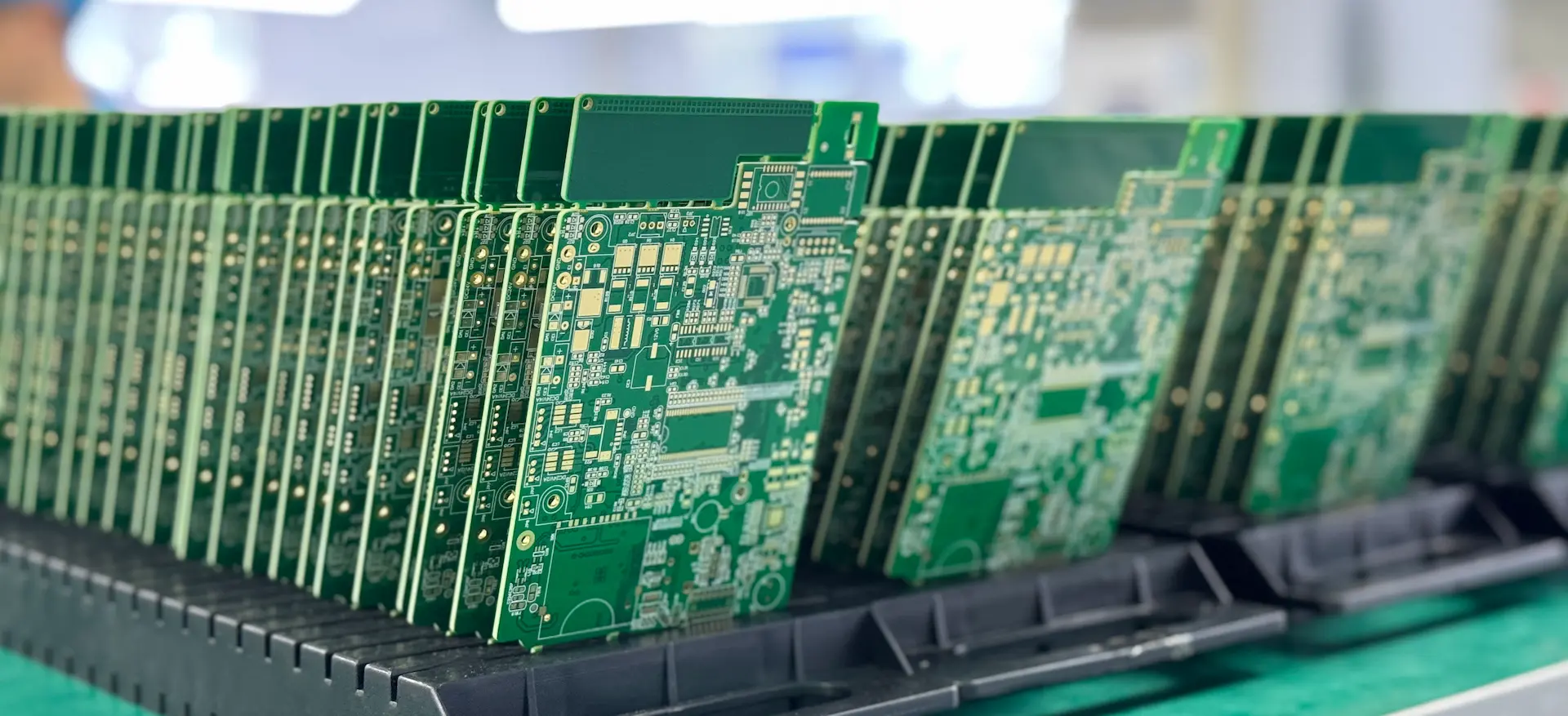
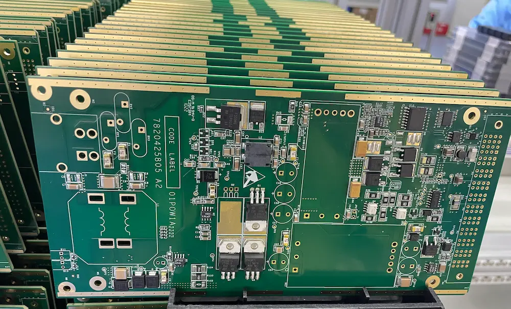
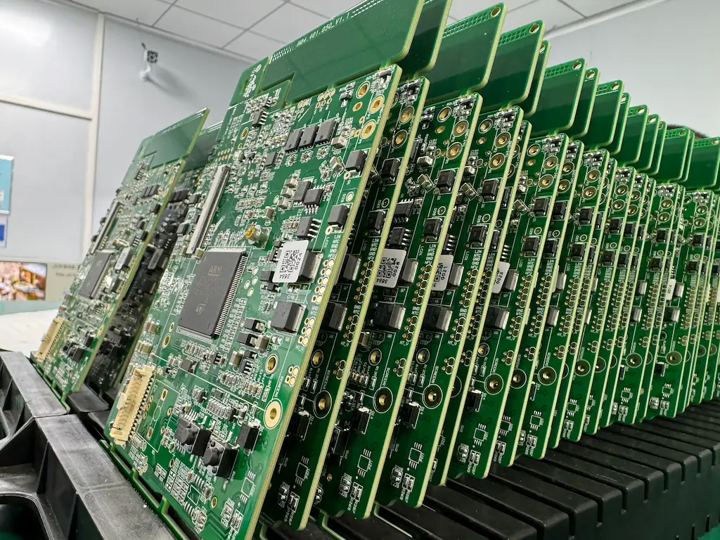
Multilayer Rigid PCB & HDI PCB Factory
From Rapid Prototype to Mass Production.
Rigid PCB prototyping and assembly with 2 to 6 day turnaround.
Certified fabrication on FR4, High Tg, and Halogen-Free rigid materials.
IPC-6012 Class 2/3 compliant rigid circuit board manufacturing with AOI, X-ray, and impedance testing.


Capabilities You Care
From standard rigid boards to complex HDI structures, we ensure our clients quality demand.
| Feature | Standard Capability | Advanced Capability |
|---|---|---|
| Layer Count | 2 - 12 Layers | Up to 30+ Layers |
| HDI Structure | N/A | 1+N+1, 2+N+2, 3+N+3, Any Layer HDI |
| Board Material | FR4 (TG135-150) | High TG (170/180), Rogers, Isola, Polyimide |
| Board Thickness | 0.4mm - 2.0mm | 0.2mm - 6.0mm |
| Copper Weight | 0.5oz - 2oz | Up to 12oz (Heavy Copper) |
| Min Trace / Space | 4mil / 4mil | 3mil / 3mil |
| Min Mech Drill | 0.2mm (8mil) | 0.15mm (6mil) |
| Min Laser Drill | N/A | 0.075mm (3mil) |
| Aspect Ratio | 8:1 | 12:1 (Thick Board) |
| Surface Finish | HASL Lead Free, Immersion Gold / ENIG | Immersion Gold / ENIG, Hard Gold, HASL Lead Free |
| Impedance Control | ±10% | ±5% Impedance coupon included per panel TDR report available upon shipment |
| Layer-to-layer registration | ≤75 μm | ≤50 μm |
| Via Plugging | Tented | VIPPO (Via-in-Pad Plated Over), Resin Plugged |
| Max Board Size | 500mm x 600mm | 1200mm x 600mm (Large Format) |
| Certifications | IATF16949, ISO13485, UL Listed | IATF16949, ISO13485, UL Listed |
Cases Study For Your Reference

12 Layers 4oz copper PCB for Automotive

10-Layer HDI (2+N+2)
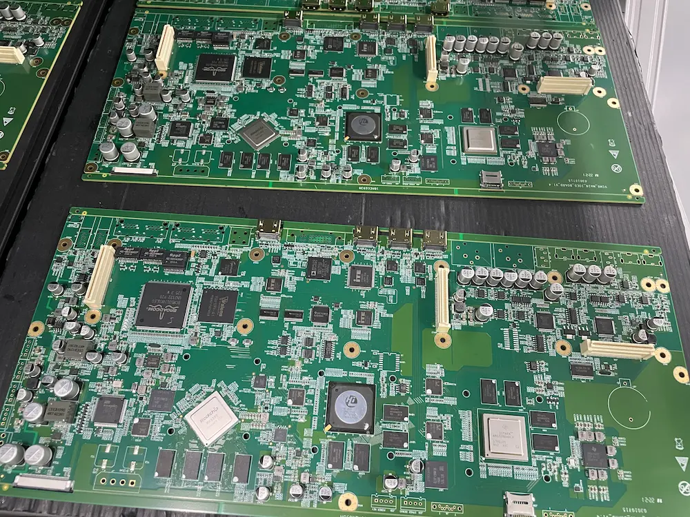
14 layers 3+N+3 HDI PCB
2OZ 8 layers PCB for Industrial Control
12 layers PCB For Motion Control
Why Partner With ACE Tech?
IPC Class 3 Standard
We don't just meet standards; we exceed them. Dedicated production lines for automotive and medical PCBs.
Quick Turnaround
24-hour expedited service for double-sided boards, 48-72 hours for multilayers. Speed without compromising quality.
Cost-Effective
Direct factory pricing with smart panelization suggestions to minimize waste and reduce your BOM cost.
Advanced Technology
Capable of 3mil trace/space, blind/buried vias, and controlled impedance for high-speed signals.
Expert Engineering
Dedicated CAM engineers review every file. We catch design errors before they become manufacturing defects.
Global Logistics
Seamless shipping to Europe and North America via DHL/FedEx/UPS, with DDP options available.
How You Order PCB
From Gerber files to your doorstep (or assembly line) in 6 simple steps.
Upload Files
Gerber RS-274X & BOM
Free DFM Check
Within 12 Hours
PCB Fabrication
Quick Turn / Mass Prod
Electrical Test
100% E-Test / AOI
FQC & Packing
Final QC / Vacuum Pack
Ship or Assembly
Global Delivery / ACE Electronics SMT Lines
Rigid & HDI PCB FAQs
Q
What is the difference between standard rigid PCB and HDI PCB?
What is the difference between standard rigid PCB and HDI PCB?
Standard rigid PCBs use through-hole vias connecting all layers, typically with larger trace widths (4mil+). HDI (High Density Interconnect) PCBs use microvias, blind/buried vias, and sequential lamination to achieve higher routing density. HDI allows for smaller pad sizes, finer traces (3mil/3mil), and enables complex designs like 1+N+1, 2+N+2, or Any Layer interconnection structures essential for smartphones and advanced automotive electronics.
Q
What layer counts do you support for rigid and HDI PCBs?
What layer counts do you support for rigid and HDI PCBs?
For standard rigid PCBs, we support 2 to 30+ layers with standard FR4 materials.
For HDI PCBs, we manufacture 4 to 20+ layer structures including 1+N+1 (standard HDI), 2+N+2 (advanced), and Any Layer HDI where every layer can interconnect to any other layer. Our maximum board size reaches 1200mm x 600mm for large format applications.
Q
What is impedance control and what tolerance do you offer?
What is impedance control and what tolerance do you offer?
Impedance control ensures signal integrity for high-speed digital and RF circuits by maintaining consistent characteristic impedance (typically 50Ω, 90Ω, or 100Ω). We offer ±5% impedance tolerance for critical applications and ±10% for standard designs. Every panel includes impedance test coupons, and we provide TDR (Time Domain Reflectometry) reports upon request. Our advanced capability supports controlled dielectric thickness and specific stack-up requirements.
Q
What materials are available for high-frequency or high-temp applications?
What materials are available for high-frequency or high-temp applications?
Beyond standard FR4 (TG135-150), we offer High TG materials (170°C/180°C) for lead-free soldering, Rogers and Isola laminates for RF/high-frequency applications, and Polyimide for extreme temperature environments. For HDI applications, we use low-Dk, low-Df materials to minimize signal loss. All materials are UL approved and suitable for automotive (IATF 16949) and medical (ISO 13485) applications.
Q
What are the typical lead times for rigid PCB prototypes?
What are the typical lead times for rigid PCB prototypes?
Standard 2-4 layer rigid PCB prototypes ship in 2-6 days. 6-8 layer boards require 5-7 days, while 10+ layer or HDI structures (1+N+1) typically take 7-10 days due to sequential lamination cycles. We offer 24-48 hour expedited services for urgent automotive and telecommunications projects. Lead times include electrical testing (100% E-test) and final inspection.
Q
What file formats do you require for PCB fabrication?
What file formats do you require for PCB fabrication?
We accept industry-standard formats including:
- Gerber RS-274X (preferred) - All copper, solder mask, silkscreen, and drill layers
- ODB++ - Contains complete stack-up and impedance information
- IPC-2581 - Modern intelligent data format
- Drill files - Excellon format (.drl) with tool definitions
We provide free DFM (Design for Manufacturing) review within 24 hours to identify potential issues before production.
Beyond Flex & Rigid-Flex PCB
From PCB fabrication to fully assembled products. Streamline your supply chain with our integrated manufacturing services.
PCB Assembly
SMT and THT assembly with 01005 component capability. Complete with AOI, X-ray inspection, and IC programming.
Explore PCBA ServicesParylene Coating
In-house CVD parylene coating for ultimate moisture and chemical protection. Ideal for medical devices and harsh environments.
Learn About Parylene CoatingBox Build Assembly
Complete electromechanical integration: enclosures, cable harnesses, PCB mounting, and functional testing to finished product.
View Box Build ServiceNeed a complete manufacturing partner?
Explore All Turnkey ServicesStart Your Projects Manufacturing Today!
Whether you need a quick quote or technical consultation, we're here to help.
Quick Response via WhatsApp
Get instant answers to your questions
Connect directly with our technical team for immediate assistance.
We typically respond within 30 minutes during business hours.
Business Hours: Mon-Fri 9:00-18:00 (GMT+8)