 ")
")
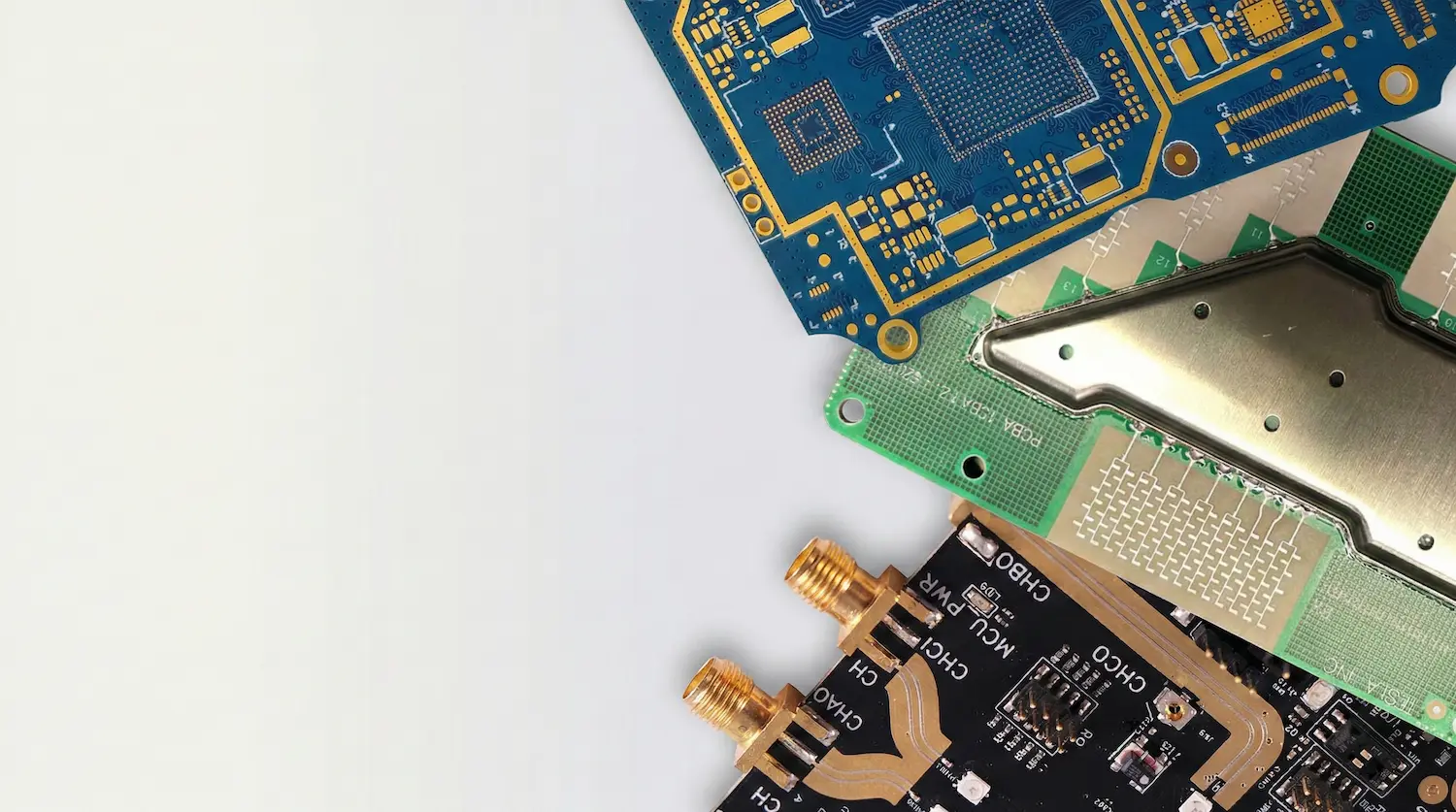
High Frequency PCB Factory
ACE Electronics offers Rogers and PTFE Teflon materials PCB

High Frequency / RF PCB
Ensuring Signal Integrity with
High-Frequency PCBs
As the frequency increases beyond a certain limit, signal losses in standard FR4 boards rise significantly. To address this, ACE Electronics offers a range of High-Frequency PCBs, designed specifically for MHz to GHz applications.
These boards utilize low-loss dielectric materials with a reduced loss tangent to minimize signal degradation, ensuring controlled electromagnetic interference (EMI) and reliable, high-speed signal transmission.
Why Choose High-Frequency Materials?
- Low Signal Loss (Df)
- Stable Dielectric (Dk)
- Controlled EMI
- MHz to GHz Support
Common Materials & Specifications
Unlike standard FR4, High-Frequency PCBs are selected based on Dk (Dielectric Constant) and Df (Dissipation Factor). The lower these values, the better the signal integrity.
Rogers Material
RO4350BDk: 3.48 @ 10GHz
Df: 0.0037
A strengthened glass hydrocarbon/ceramic laminate. Features low Z-axis CTE for stable multilayer circuits.
High-frequency power amplifiers & Multilayer designs.
PTFE Teflon
ZYF SeriesDk: 2.55 - 3.0
Df: 0.0016 - 0.0019
Outstanding comprehensive performance. Excellent temperature resistance, heat dissipation, and mechanical stability.
High-complexity, high-reliability & Cost-effective designs.
Specialized in Rogers RO4350B & PTFE Teflon Laminates.
ACE Electronics High-Frequency & RF Capabilities
Precision engineering for Signal Integrity. From standard Rogers cores to complex Hybrid Stack-ups and mmWave solutions.
Inventory & Speed
We stock standard cores and prepregs to expedite your RF prototypes.
Rogers Corporation
- RO4350B / RO4003C Power Amps
- RO3003 / RO3006 77GHz Radar
- RO4835 High Stability
Isola Group
- I-Speed / Astra MT77 mmWave
- TerraGreen Ultra-low loss
Panasonic
- Megtron 6 (R-5775)
- Gold standard for High-Speed Digital (Servers)
Taconic
- TLX / RF-35
- Cost-effective PTFE solutions
High-Frequency PCB Validation
Beyond Connectivity — Ensuring Signal Fidelity
Controlled Impedance & Reflection
Method
TDR-based impedance verification using dedicated RF test coupons.
Validated Parameters
- Characteristic impedance (50 Ω / differential lines)
- Impedance uniformity across panel
- Correlation to S11 return loss
Tolerance
Broadband S-Parameter Characterization
Method
Vector Network Analyzer measurement up to 40 GHz.
What We Validate
- Insertion loss (S21) vs frequency
- Return loss (S11)
- Phase stability / group delay
- Correlation with laminate Dk / Df models
Low-PIM Qualification
Application Specific
Applies to
Base-station antennas & High-power passive RF structures
Capability
PIM performance down to -155 dBc / -163 dBc
Focus Areas
- Surface finish metallurgy
- Copper oxidation control
- Mechanical contact integrity
Micro-Section & Material Integrity
Purpose
Verify the physical consistency behind electrical performance.
Inspection Includes
- Dielectric thickness vs stack-up design
- Copper profile & roughness correlation to conductor loss
- Via plating integrity & resin recession control
- PTFE hybrid lamination quality
Cleanliness & Long-Term Reliability
Cleanliness Standard
- IPC-TM-650 ionic contamination compliance
- Rose test / Omegameter verification
Extended RF Reliability (when required)
- Thermal cycling stability
- Moisture impact on dielectric properties
- CAF resistance for high-voltage RF environments
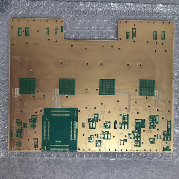
Cases Study For Your Reference

RO4350B + FR4 Tg170 PCB

Rogers PCB
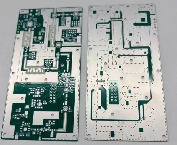
Roger4350B + FR4 Immersion Silver
Why Partner With ACE Tech?
IPC Class 3 Standard
We don't just meet standards; we exceed them. Dedicated production lines for automotive and medical PCBs.
Quick Turnaround
24-hour expedited service for double-sided boards, 48-72 hours for multilayers. Speed without compromising quality.
Cost-Effective
Direct factory pricing with smart panelization suggestions to minimize waste and reduce your BOM cost.
Advanced Technology
Capable of 3mil trace/space, blind/buried vias, and controlled impedance for high-speed signals.
Expert Engineering
Dedicated CAM engineers review every file. We catch design errors before they become manufacturing defects.
Global Logistics
Seamless shipping to Europe and North America via DHL/FedEx/UPS, with DDP options available.
How You Order PCB
From Gerber files to your doorstep (or assembly line) in 6 simple steps.
Upload Files
Gerber RS-274X & BOM
Free DFM Check
Within 12 Hours
PCB Fabrication
Quick Turn / Mass Prod
Electrical Test
100% E-Test / AOI
FQC & Packing
Final QC / Vacuum Pack
Ship or Assembly
Global Delivery / ACE Electronics SMT Lines
High Frequency PCB FAQs
Q
What makes High Frequency PCBs different from standard FR4 boards?
What makes High Frequency PCBs different from standard FR4 boards?
High Frequency PCBs use specialized low-loss materials (like Rogers, Taconic, or Isola) instead of standard FR4 epoxy. These materials maintain stable dielectric constant (Dk) and low dissipation factor (Df) at frequencies above 1GHz, ensuring minimal signal attenuation. They feature tighter impedance tolerances (±5%), smoother copper surfaces (RTF/VLP copper), and hybrid constructions combining RF materials with standard FR4 for cost optimization.
Q
Which materials do you recommend for 5G and millimeter-wave applications?
Which materials do you recommend for 5G and millimeter-wave applications?
For 5G sub-6GHz: Rogers RO4350B (Dk 3.48, Df 0.0037) or RO4003C offer excellent cost-performance balance.
For mmWave (24GHz+): Rogers RO3003 (Dk 3.0, Df 0.0013), Taconic TLY-5, or Isola I-Tera MT40 provide ultra-low loss characteristics.
For hybrid designs, we combine RF materials on outer layers with standard FR4 cores to reduce costs while maintaining signal integrity in critical trace areas.
Q
How do you ensure impedance control for RF and microwave signals?
How do you ensure impedance control for RF and microwave signals?
We maintain ±5% impedance tolerance through precision controlled depth routing, laser direct imaging (LDI), and automated optical inspection (AOI). For critical RF traces, we use 3D electromagnetic field solvers (Polar, Si8000) during design validation. Each production panel includes TDR (Time Domain Reflectometry) test coupons, and we provide S-parameter measurement reports up to 40GHz using vector network analyzers (VNA) upon request.
Q
What surface finishes work best for high-frequency applications?
What surface finishes work best for high-frequency applications?
ENIG (Electroless Nickel Immersion Gold) is preferred for most HF applications due to its flat surface and stable contact resistance. For mmWave applications above 30GHz, we recommend Immersion Silver or OSP (Organic Solderability Preservative) to avoid the "skin effect" losses associated with nickel. Selective hard gold plating is available for edge connectors requiring repeated mating cycles in RF test environments.
Q
What are the typical applications for your High Frequency PCBs?
What are the typical applications for your High Frequency PCBs?
Our HF PCBs serve 5G base stations and CPE devices, automotive radar (77GHz ADAS systems), satellite communications (Ku/Ka band), RFID readers, and high-speed data centers (100G/400G networking).
We also manufacture boards for medical imaging (MRI coils), microwave test equipment, and aerospace/defense systems requiring ITAR compliance and rigorous environmental testing.
Q
How do you handle thermal management in high-frequency designs?
How do you handle thermal management in high-frequency designs?
High-frequency circuits generate significant heat due to conductor losses. We implement thermal vias and copper coin insertion for power amplifier modules. For extreme thermal requirements, we offer Metal Core HF PCBs combining Rogers RO4000 series with aluminum bases, or ceramic-filled thermally conductive laminates. Thermal simulation and TML (Thermal Management Layer) designs ensure consistent performance across -40°C to +150°C operating ranges.
Beyond High Frequency PCB
From PCB fabrication to fully assembled products. Streamline your supply chain with our integrated manufacturing services.
PCB Assembly
SMT and THT assembly with 01005 component capability. Complete with AOI, X-ray inspection, and IC programming.
Explore PCBA ServicesParylene Coating
In-house CVD parylene coating for ultimate moisture and chemical protection. Ideal for medical devices and harsh environments.
Learn About Parylene CoatingBox Build Assembly
Complete electromechanical integration: enclosures, cable harnesses, PCB mounting, and functional testing to finished product.
View Box Build ServiceNeed a complete manufacturing partner?
Explore All Turnkey ServicesStart Your Projects Manufacturing Today!
Whether you need a quick quote or technical consultation, we're here to help.
Quick Response via WhatsApp
Get instant answers to your questions
Connect directly with our technical team for immediate assistance.
We typically respond within 30 minutes during business hours.
Business Hours: Mon-Fri 9:00-18:00 (GMT+8)